
HALUKKILINCER.COM · Sectors
Semiconductors
Fab, packaging, materials, and test constraints that set the pace behind advanced logic and power devices.
67 analyses
Semiconductors
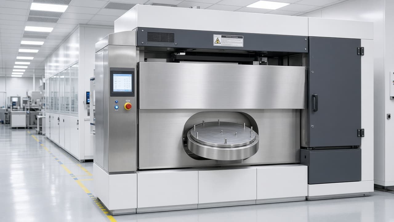
PEB hot-plate uniformity owns CD swings the scanner dose knob cannot erase
Post-exposure bake finishes the latent image. Plate temperature range across the wafer rewrites line width while exposure energy still looks centered. Track bake metrology beats another dose ladder.
30 Sept 2026
Semiconductors
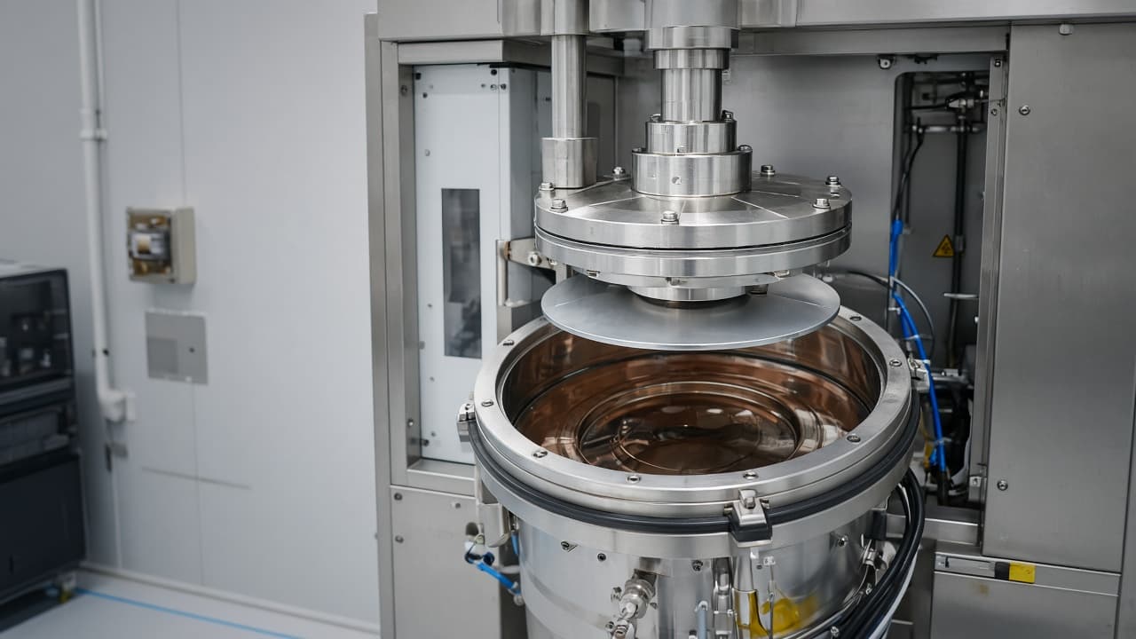
Copper ECD inherits the seed—thin or patchy seed becomes plating voids and thickness chaos
Electrochemical deposition needs a continuous conductive seed. PVD or CVD seed thickness, voids, and edge thinning rewrite fill quality before bath chemistry gets the blame.
29 Sept 2026
Semiconductors
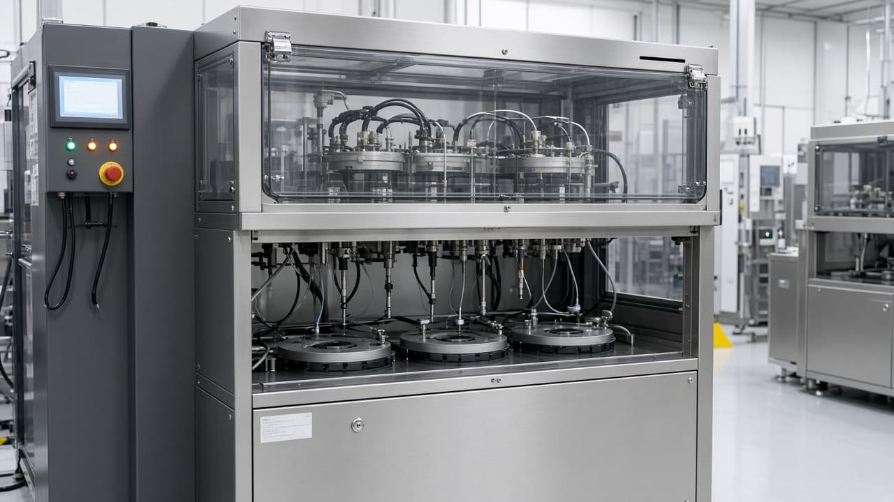
BARC thickness owns the lithography window the resist recipe cannot fix
Bottom anti-reflective coating sets reflectivity and swing-curve behavior under the photoresist. Track coat uniformity and post-apply bake drift rewrite CD and focus budgets before the scanner exposure dose looks wrong.
28 Sept 2026
Semiconductors
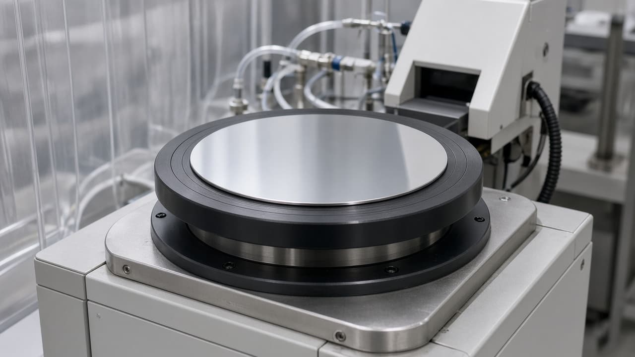
Spin-chuck vacuum loss throws wafers before the recipe looks wrong
Track coaters and related tools hold the wafer on vacuum grooves. Plugged ports, worn seals, and soft vacuum make the disk skate or fly while the recipe timer still claims a perfect coat.
26 Sept 2026
Semiconductors
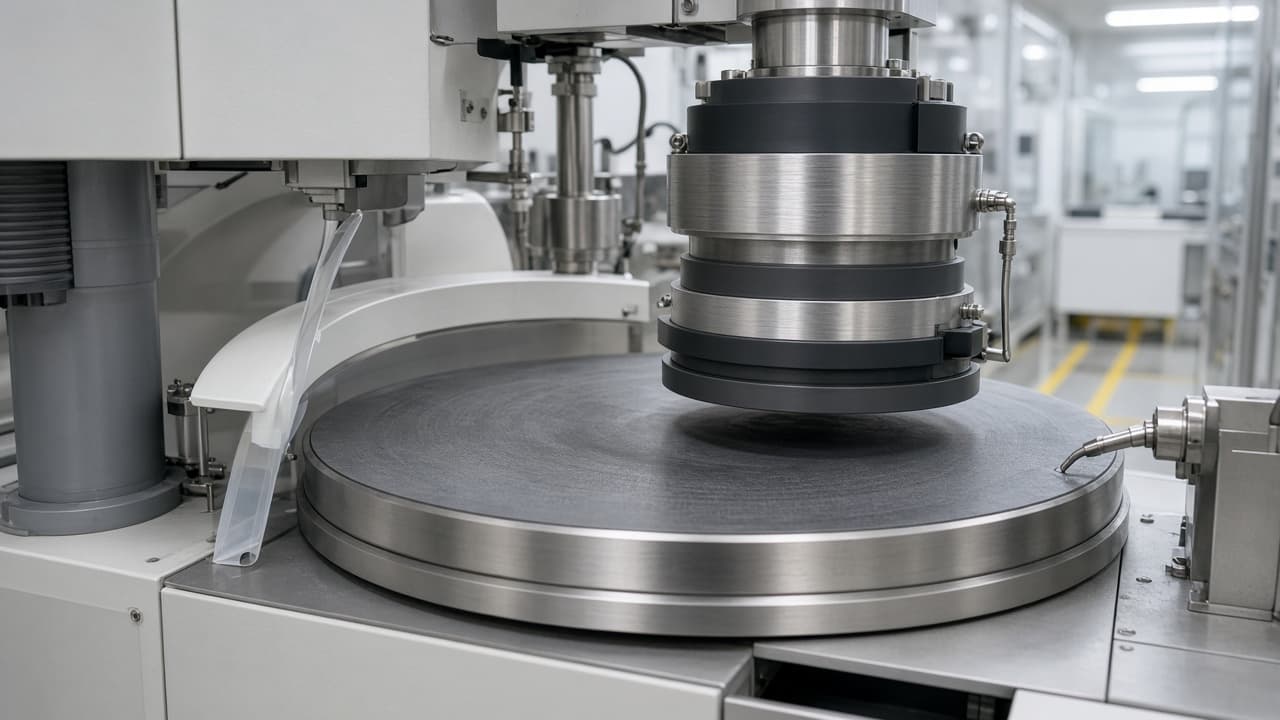
Copper CMP does not fail as ‘pad looks shiny’—it fails as dishing and erosion maps
Overpolish clears residual copper and then keeps cutting soft metal in wide features while barriers hold. Dishing, erosion, and endpoint honesty decide whether the next lithography step inherits a topography problem.
25 Sept 2026
Semiconductors
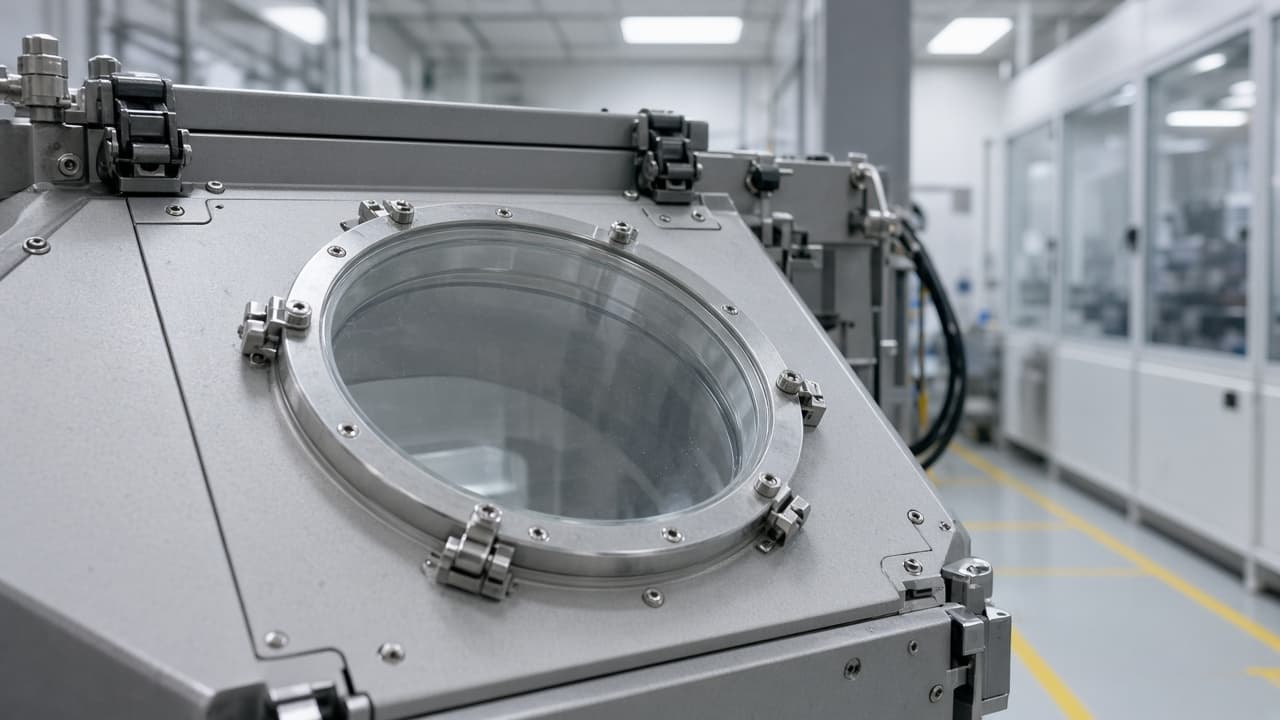
Etch optical endpoint fails quietly when the quartz viewport clouds
Endpoint detectors watch light through a window. Polymer haze, etch by-product film, and a misaligned fiber turn a clear endpoint into a timed over-etch or an early abort that scrapes yield without a hard alarm.
22 Sept 2026
Semiconductors
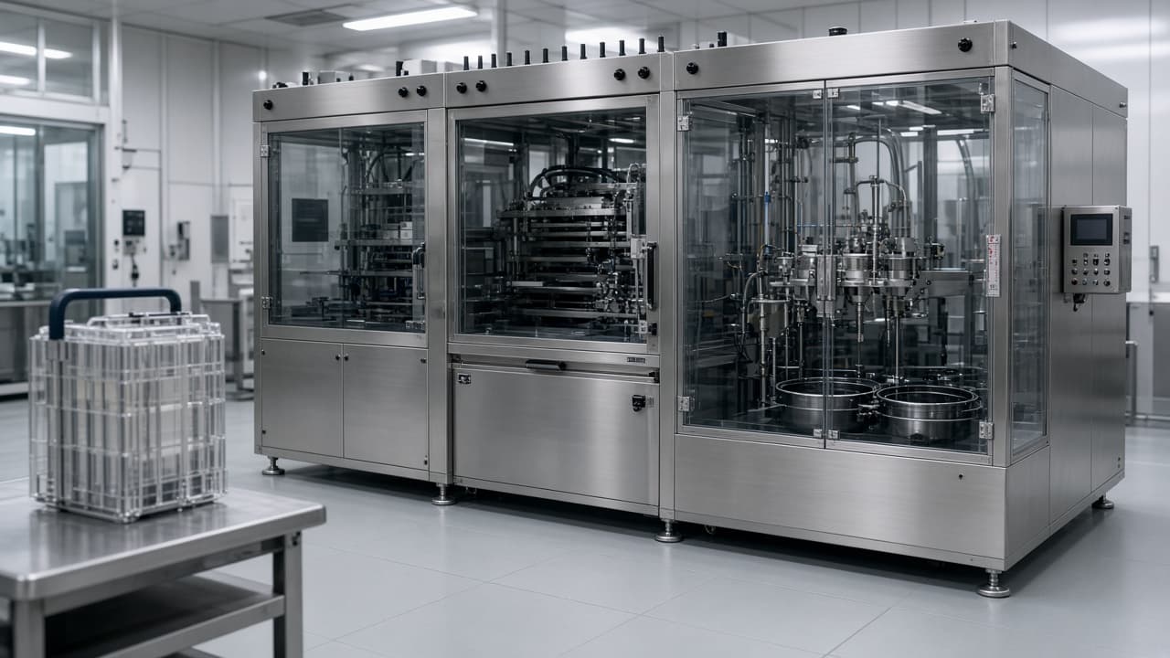
Edge-bead removal owns the wafer rim that coater tracks leave thick—and etch modules inherit
EBR solvent, nozzle aim, and spin recipe decide whether photoresist piles at the edge become particles and edge-die scrap. Bevel etch and ash strip are later chapters; this one is the track’s edge cut.
21 Sept 2026

Semiconductors
RF matching networks keep etch stable—reflected power is the first confession that the match drifted
Tune capacitors, cable integrity, and chamber load decide whether forward power reaches the plasma. MFC zero/span and cryopump notes are other modules; this one is match health and reflected-power honesty.
19 Sept 2026

Semiconductors
Mass flow controllers set etch and CVD stoichiometry—zero and span drift rewrite the recipe without touching the recipe editor
Thermal and pressure-based MFCs report what their calibration last believed. Gas correction factors, zero offsets, and overdue span checks move film thickness and etch rate before anyone opens the process recipe.
19 Sept 2026
Semiconductors
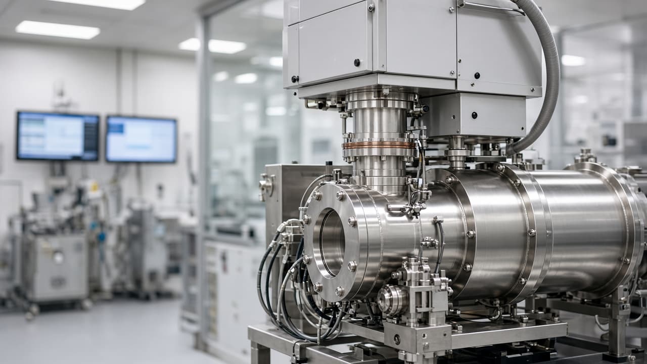
Cryopumps do not fail as ‘bad vacuum’—they fail when regeneration never restores capacity
On etch and CVD tools, cryopumps trap water and process gases on cold arrays. Base pressure recovers after regen only if the array still has capacity and the foreline still pulls. Skipping regen to save takt poisons the next recipe quietly.
18 Sept 2026
Semiconductors
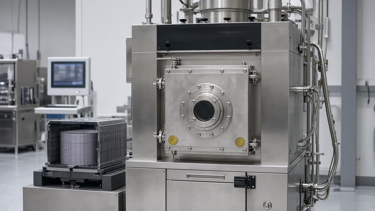
Bevel etch owns the wafer edge that every other module pretends is someone else’s problem
Frontside etch, CMP, and lithography assume a controlled bevel and exclusion zone. Particles and films left on the edge migrate inward; tools that never ‘own’ bevel still inherit its scrap.
17 Sept 2026
Semiconductors
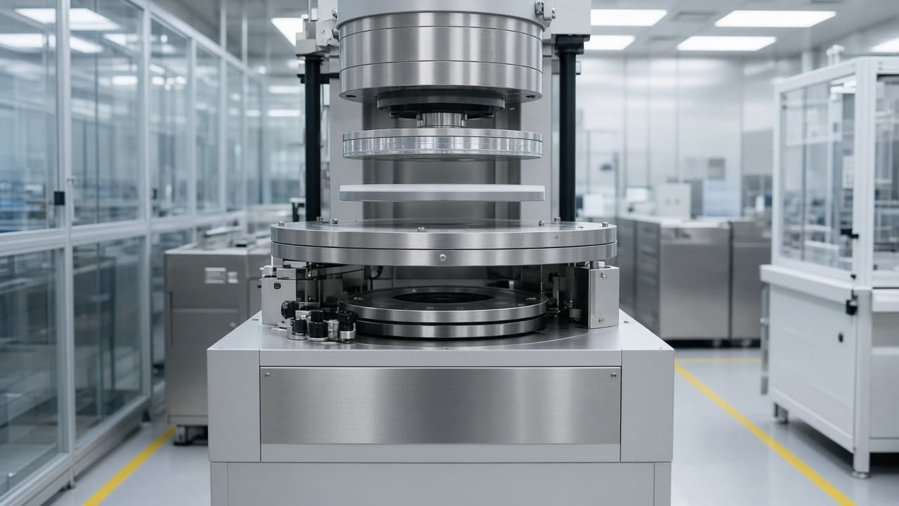
Temporary wafer bonding is a handle for thinning—debond yield decides whether the handle was worth it
Carrier attach, adhesive or release layers, and debond method enable backside processing on fragile wafers. Particles, voids, and residual adhesive after release show up as yield and contamination long after the bond tool looks idle.
15 Sept 2026

Semiconductors
ALD film thickness drifts when precursor delivery temperature and line heat tracing are treated as utilities footnotes
Ampoule setpoints, heated transfer lines, and vapor-draw stability decide whether atomic layer deposition sees a steady precursor dose. Chamber recipe screens cannot compensate for a cold spot that condenses vapor upstream.
14 Sept 2026

Semiconductors
Sputter target life is an erosion map, not only a kilowatt-hour counter on the tool
Racetrack depth, redeposition, and thickness uniformity drift long before the target ‘looks finished.’ Chambers that change targets only on calendar risk both scrap and wasted metal.
11 Sept 2026
Semiconductors
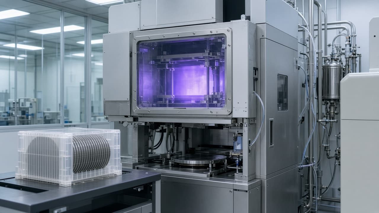
Incomplete photoresist strip after plasma ash still shows up two modules later
Endpoint signals and optical residues decide whether ash cleaned the wafer or only cleared the chamber recipe timer. Downstream etch and implant inherit carbon the strip step was supposed to remove.
10 Sept 2026
Semiconductors
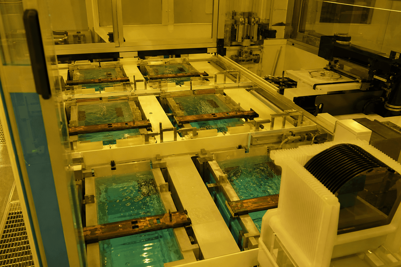
Copper ECD fails as bath and current density honesty—not as a ‘plating tool green’ lamp
Additive health, anode state, flow, and within-wafer current distribution decide seed and fill uniformity. A tool that finishes every lot on schedule can still ship thickness maps that kill the next CMP or etch window.
08 Sept 2026

Semiconductors
A green particle count can lie for months if the counter’s baseline drifts while the room does not
ISO 21501 cal intervals, inlet hose cracks, and laser aging shift zeros before fab yield moves. Qualifying a bay on a drifting instrument is paperwork clean, not air clean.
27 Aug 2026
Semiconductors
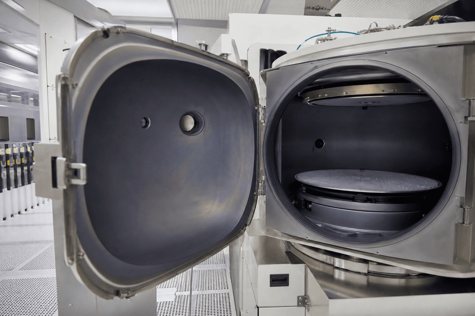
First-wafer effect is chamber-wall memory after wet clean, not a mystery RF hour
Seasoning wafers, polymer on walls, and the first production lot after PM decide whether etch rate and selectivity match the POR—or only the meeting notes. A green base-pressure icon does not certify a naked chamber.
26 Aug 2026
Semiconductors
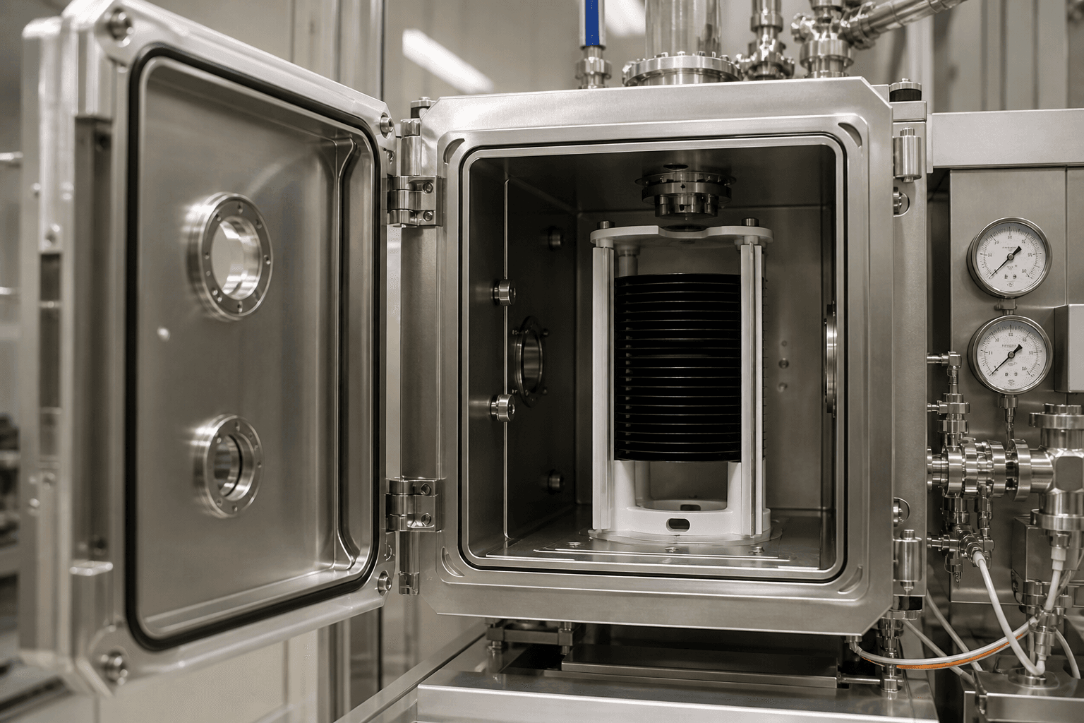
Load-lock leak-up decides whether the chamber meets the next recipe or the hallway
Crossover pressure, door seal wear, and pumpdown time to base decide whether a transfer is vacuum-clean—or a slow leak that poisons the next recipe. A green chamber pressure icon does not certify the leak-up curve from the last PM.
26 Aug 2026
Semiconductors
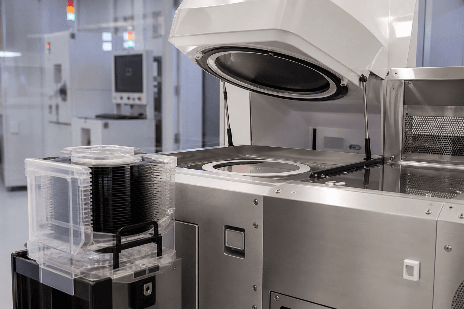
Spin-rinse dryer watermarks are rinse chemistry and spin truth, not a mystery etch bias
DI quality, IPA or surface-tension aids, exhaust, and recipe spin profiles decide whether a wet clean leaves a dry wafer—or rings and spots that look like particles and kill yield at inspection. A green particle counter on the DI loop does not certify the last twenty seconds of the dry.
25 Aug 2026
Semiconductors
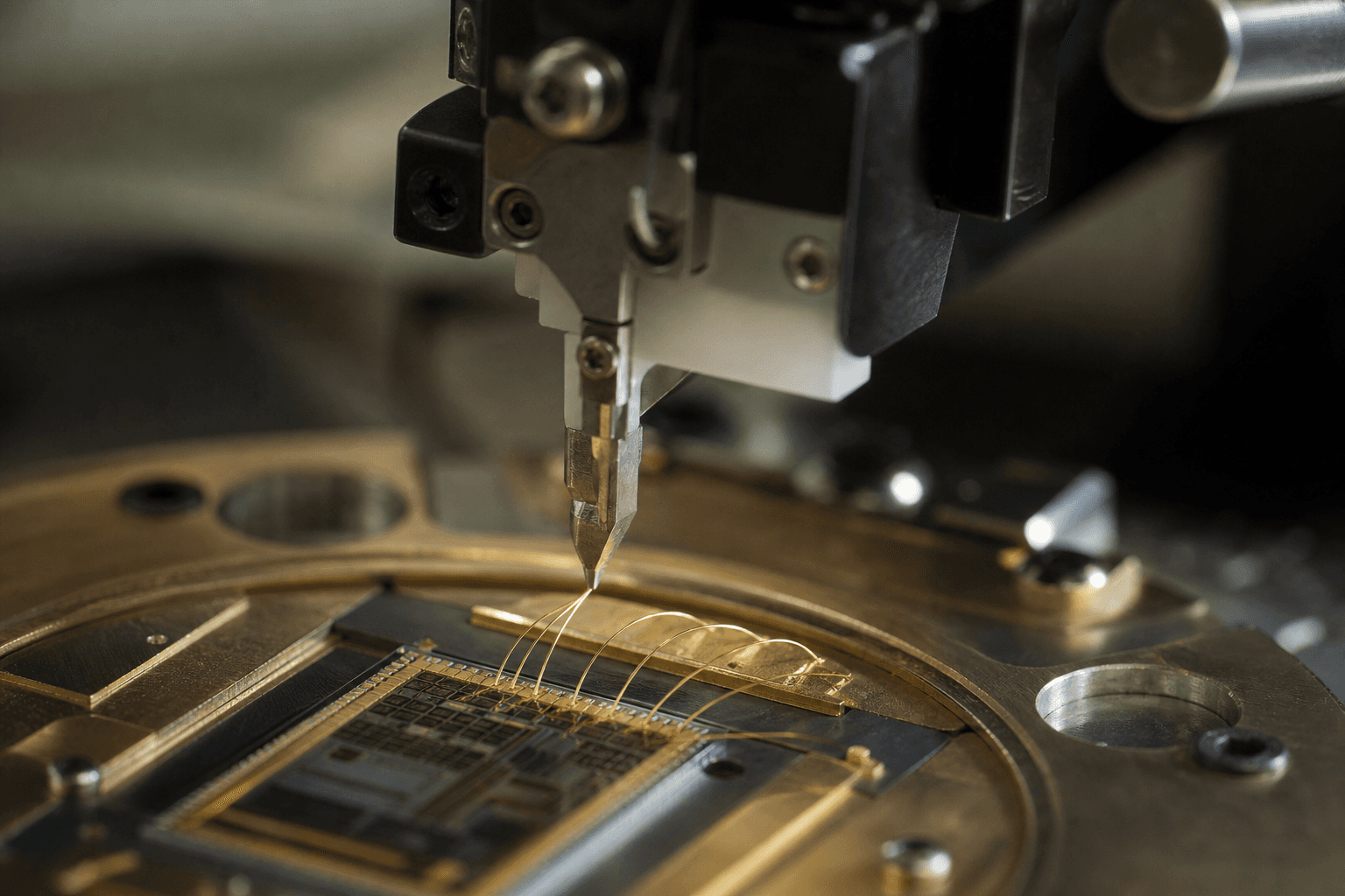
Wire-bond yield cliffs are capillary face and second-bond truth, not a mystery mold compound
Capillary wear, chamfer geometry, and stitch/ball parameters decide whether pads lift or necks break long after the die attach looked green. A stable wire spool lot does not certify the tip that has fired a hundred thousand bonds.
24 Aug 2026
Semiconductors
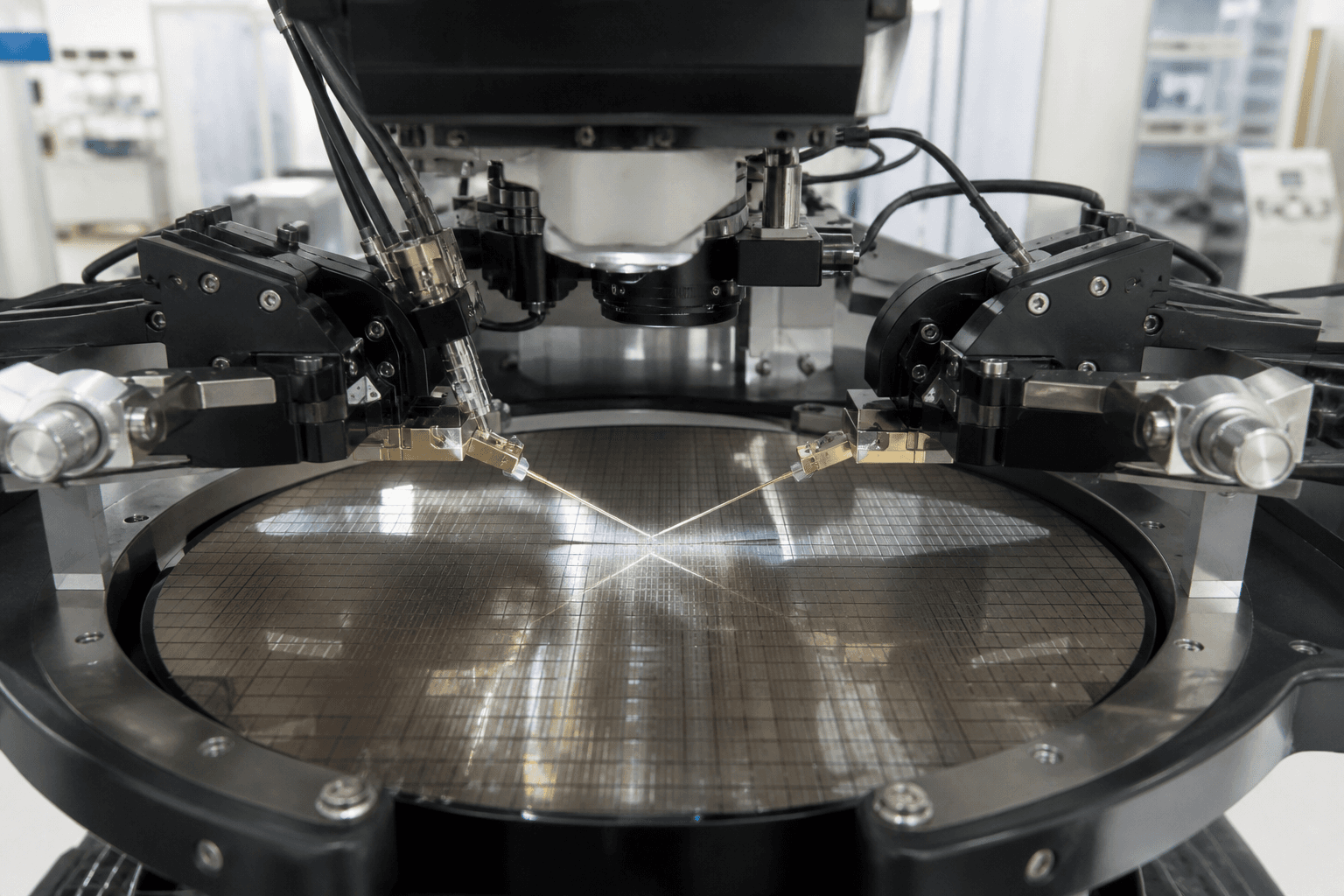
Wafer-sort yield cliffs are often probe-card contact, not a new etch bias
Pogo and needle wear, planarity, and scrub length decide whether a die fails open in sort or passes and dies in package. A green fab lot history does not certify the card that has touched a hundred thousand touchdowns.
22 Aug 2026
Semiconductors
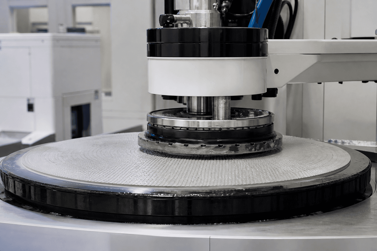
CMP pads fail as groove memory and conditioner truth, not as a slurry tote label
Pad groove depth, glaze, and diamond conditioner aggressiveness decide removal rate and within-wafer uniformity after the slurry lot is already accepted. A green particle-size certificate does not certify the pad that has been polishing for three thousand wafers.
21 Aug 2026
Semiconductors
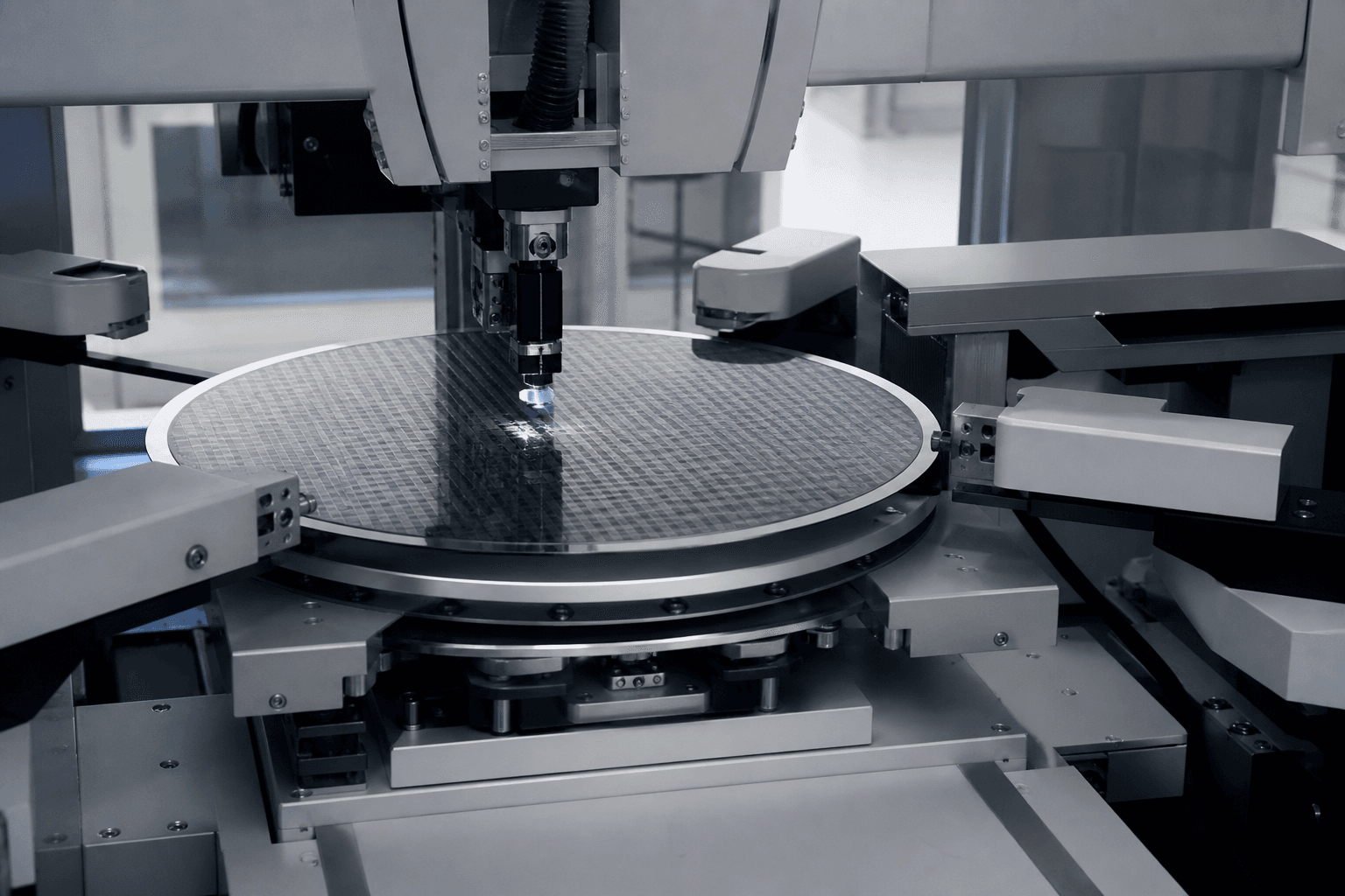
Wafer bow is a lithography input, not a metrology afterthought
Global and local warp decide focus budget, overlay, and chuck contact long before the scanner recipe is blamed. A fab that only measures bow after a yield crisis is paying for rework that a gate at the incoming or post-film step would have stopped.
21 Aug 2026
Semiconductors
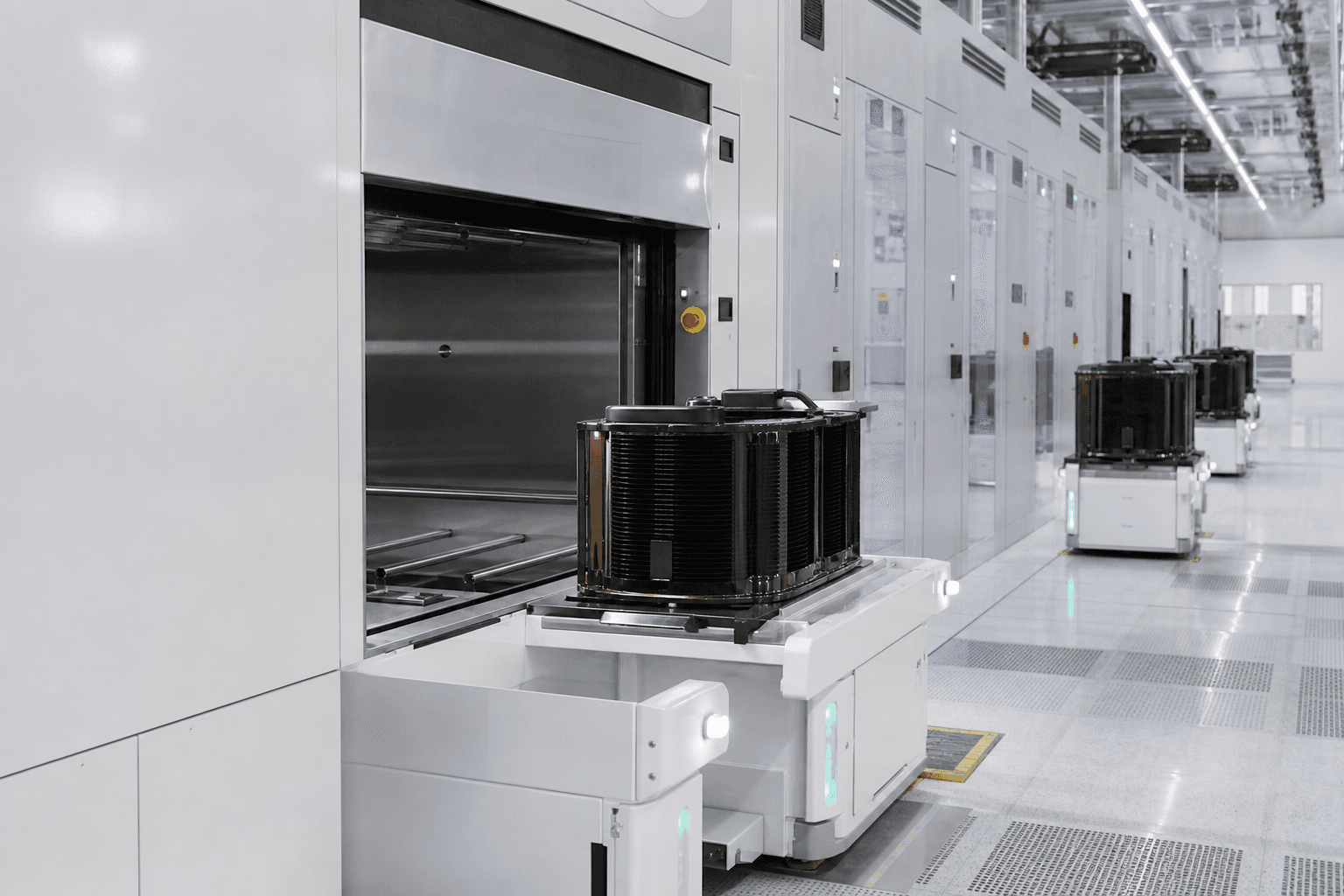
Q-time between etch and film is a yield clock, not a dispatch inconvenience
Queue time after plasma etch lets residues, oxides, and airborne molecular contamination rewrite the surface the next tool thinks it owns. Dispatch that maximizes tool utilization without a hard Q-time inhibit is choosing wafers that look on-time and die that fail later.
19 Aug 2026
Semiconductors
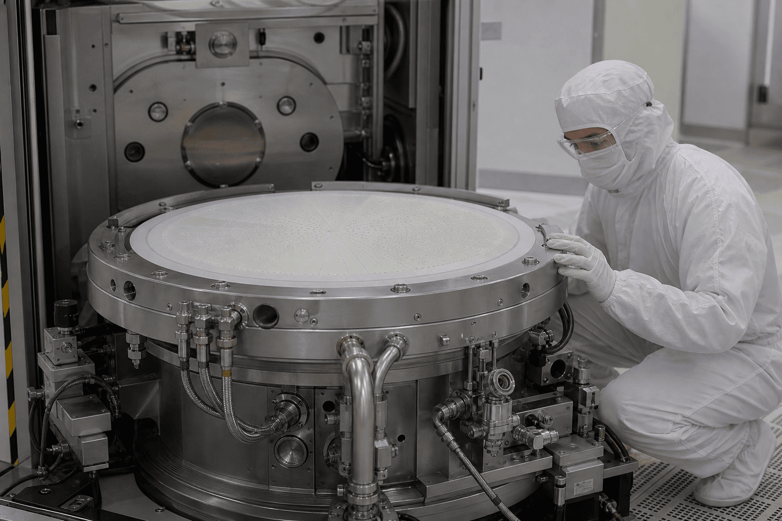
ESC helium leaks look like etch bias until someone sniffs the chuck
Backside helium pressure, leak-up rate, and dechuck behavior decide wafer temperature uniformity on plasma tools. When the ceramic chuck or the lift-pin seals leak, the recipe still runs—edge CD and overlay just wander, and the fault is filed under chamber matching.
19 Aug 2026
Semiconductors
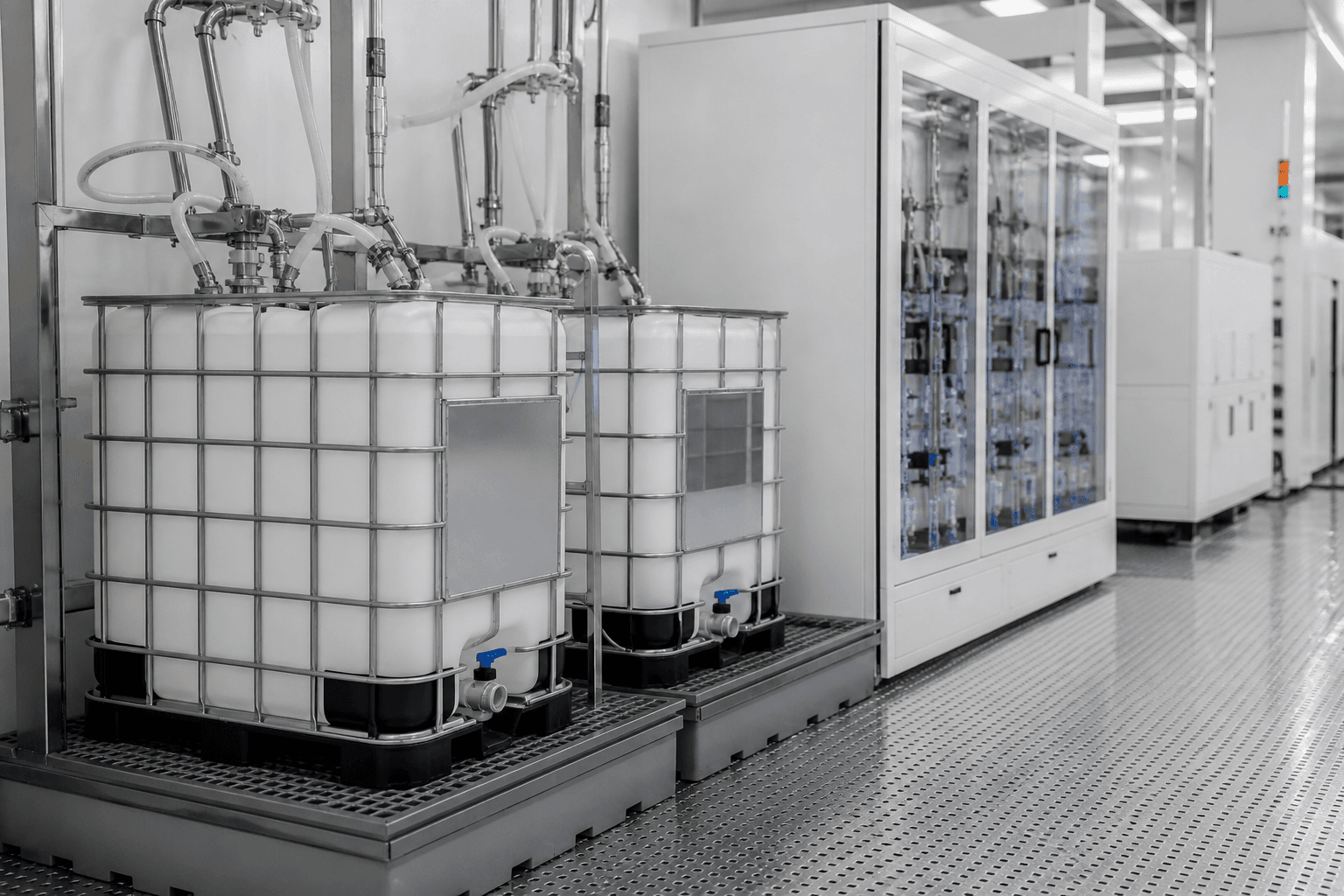
CMP slurry is a chemical supply chain before it is an abrasive
Particle size distribution, pH stability, and cold-chain integrity decide whether chemical mechanical planarization delivers the flat wafer the next process step expects—or introduces the micro-scratch population that inspection cannot always catch before device test.
18 Aug 2026
Semiconductors
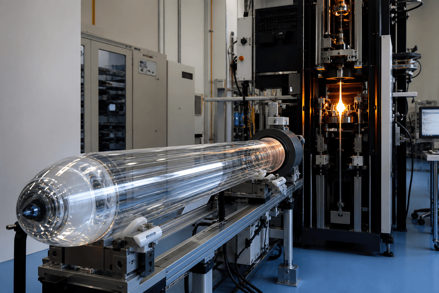
AI campus fiber demand starts upstream in preform glass—not in the patch-panel brochure
Preform quality, draw yield, and specialty fiber capacity decide whether datacenter optical builds can scale—materials and draw-plant truth behind AI fabrics, not CPO package demos alone, not glass-core substrate packaging races, not liquid-cooling rack essays.
13 Aug 2026
Semiconductors
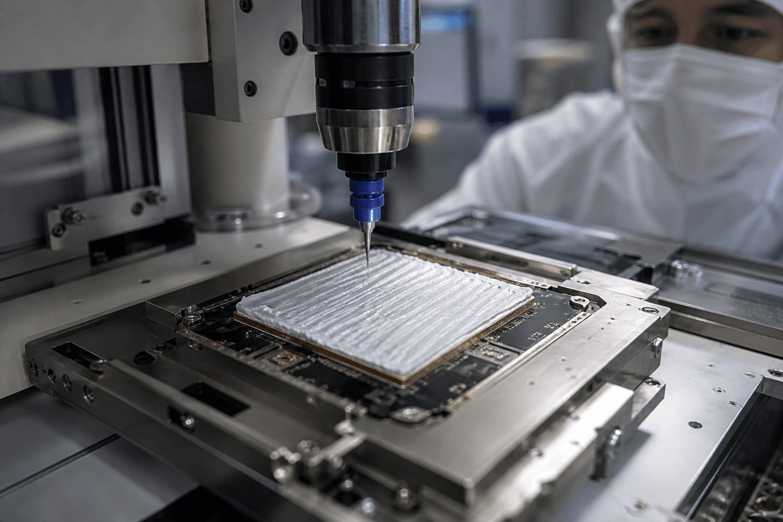
TIM bond-line control is the quiet thermal gate under AI module lids
Paste pattern, bond-line thickness, and void rules decide whether lid attach cools silicon—or cooks it—semiconductor packaging thermal process, not liquid-cooling rack facilities alone, not silver sinter die attach alone, not molded underfill voids alone.
11 Aug 2026
Semiconductors
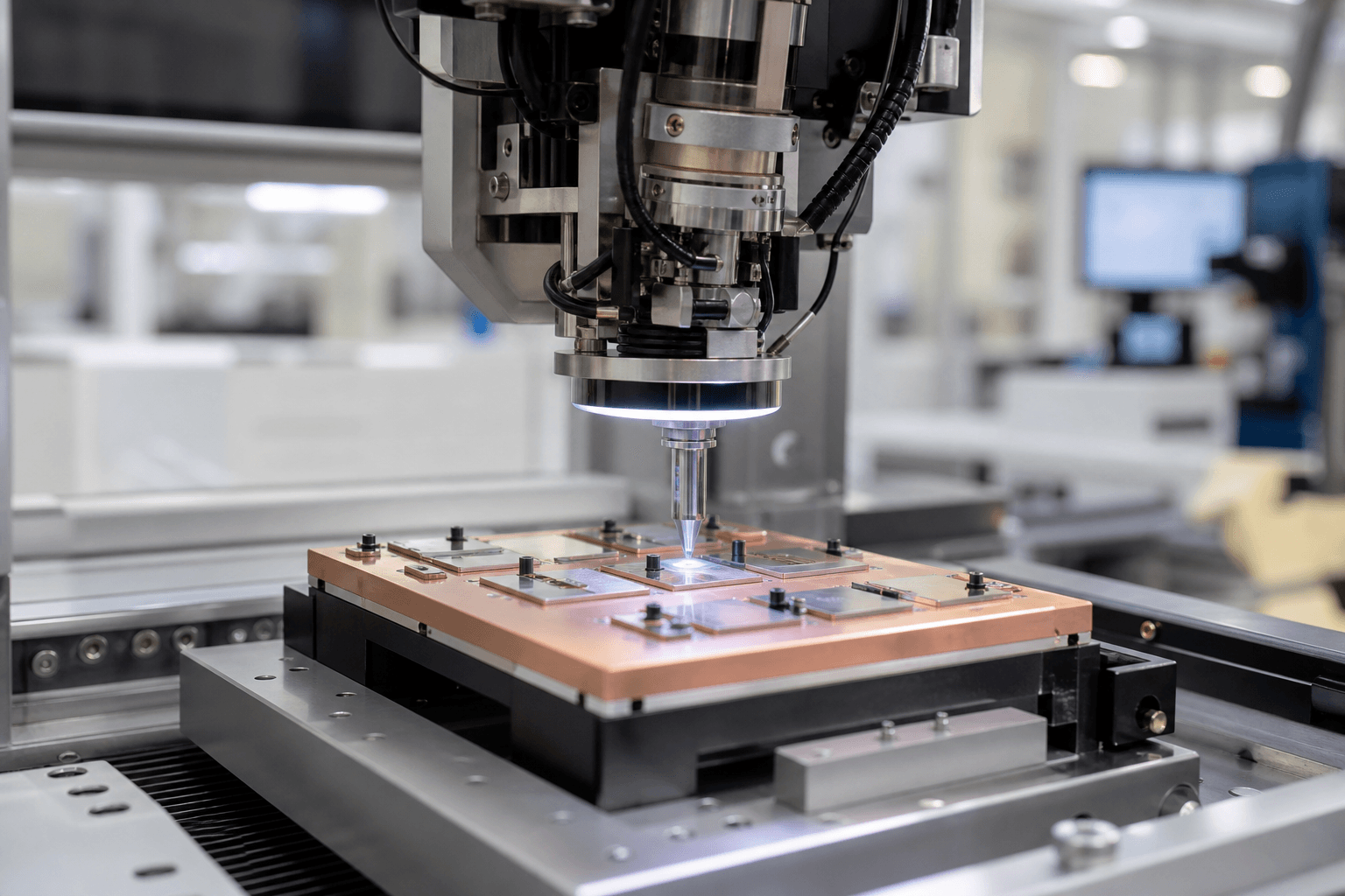
Silver sinter die attach becomes the thermal gate for power modules
Bond-line thickness, sinter voids, and pressure-temperature profiles decide whether SiC/GaN modules survive heat—semiconductor power packaging process, not hybrid-bond HBM stacks, not molded underfill voids alone, not package burn-in throughput.
10 Aug 2026
Semiconductors
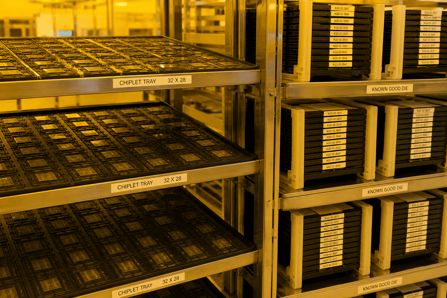
Known-good-die inventory is the chiplet schedule nobody puts on the packaging slide
KGD bins, tray genealogy, and test-escape economics decide whether multi-die packages can start—semiconductor packaging operations, not UCIe protocol decks alone, not hybrid-bond yield alone, not ABF substrate capacity alone.
08 Aug 2026

Semiconductors
HVLP copper foil becomes the PCB gate after glass fabric stops being the only villain
Foil grades, processing fees, and qualification cycles decide whether AI and HDI boards can be built—semiconductor/electronics materials supply, not ABF substrate capacity alone, not glass-core package races, not CMP slurry logistics.
07 Aug 2026
Semiconductors
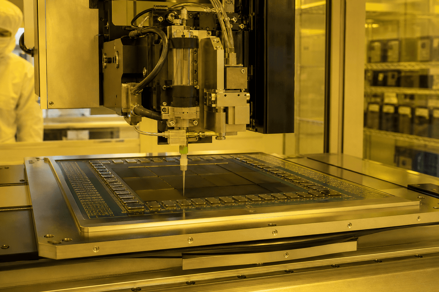
Molded underfill voids become the quiet killer after the bonding slide is green
Fillet geometry, cure profiles, and void metrology decide whether large AI packages survive thermo-mechanical life—semiconductor packaging process control, not hybrid-bond yield decks, not substrate warpage alone, not burn-in throughput gates.
05 Aug 2026
Semiconductors
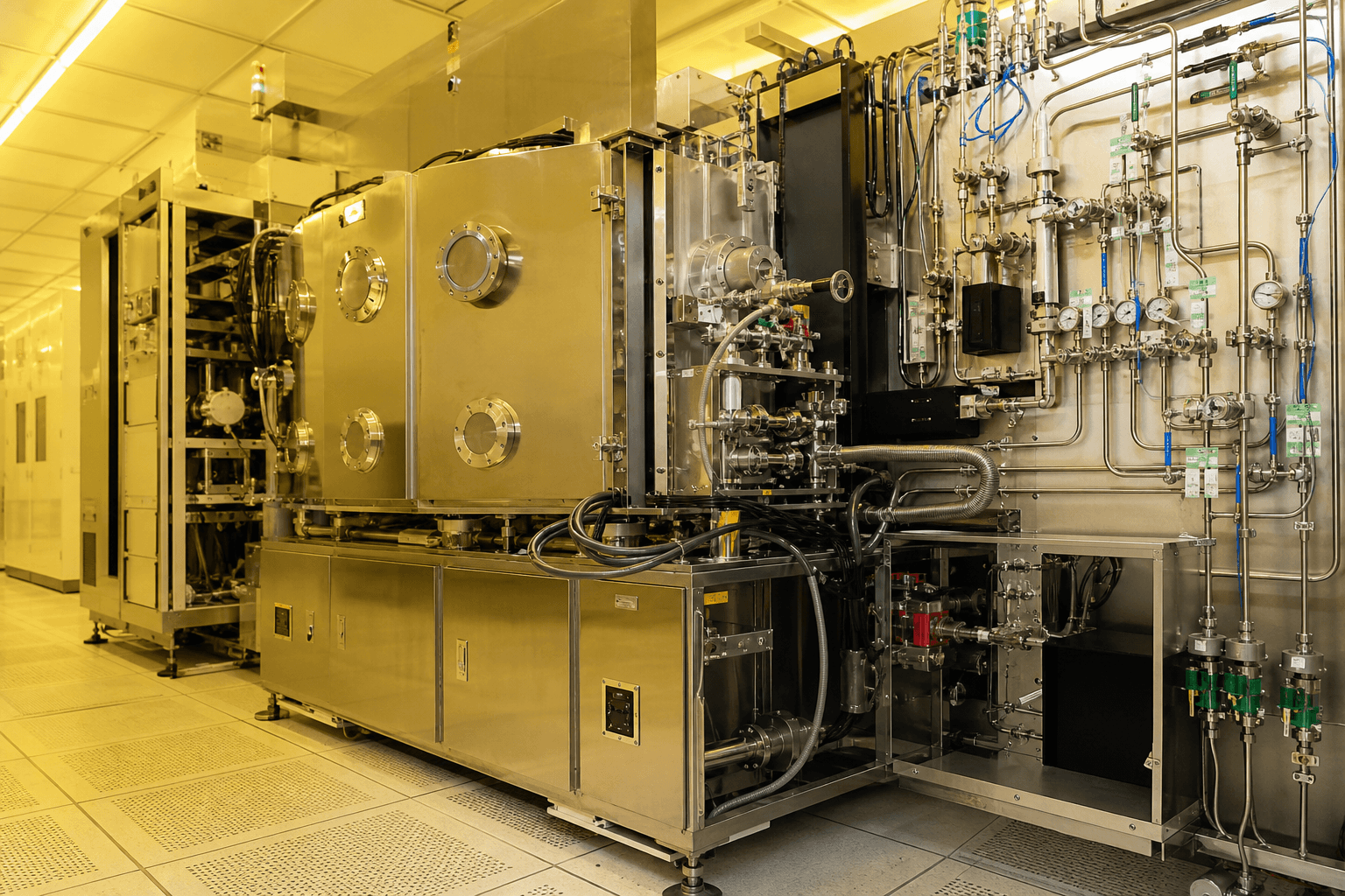
SiC epitaxy defect maps decide which wafers deserve a device lot
Epi thickness uniformity, killer-defect density, and disposition maps sit between crystal wafers and power devices—semiconductor process control, not boule supply headlines, not SiC/GaN switch marketing, not package burn-in gates.
05 Aug 2026
Semiconductors
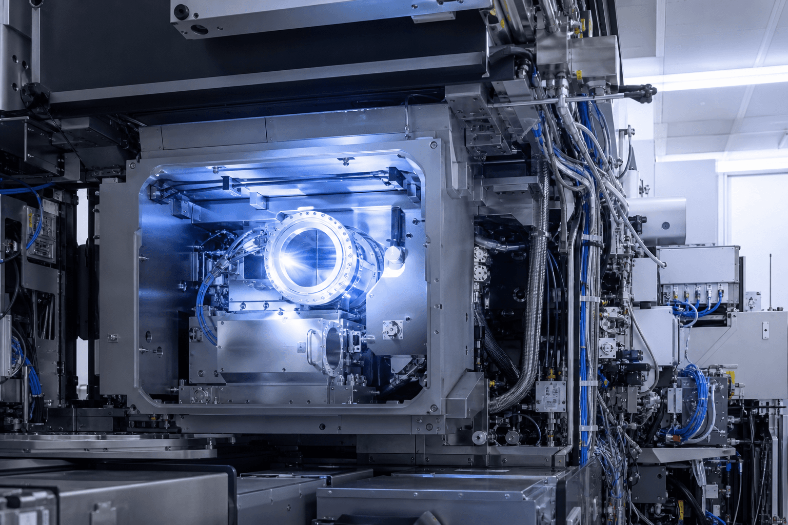
Source calendar EUV-S7: green days that were not productive days
Available hours, dose stability, and collector state decide whether ‘up’ means wafers—semiconductor EUV source calendar, not High-NA stitching essays, not reticle custody chains, not chamber matching scorecards.
05 Aug 2026

Semiconductors
Reticle custody RC-6: the mask that left the cage without a name
Checkout signatures, pod IDs, and return metrology decide whether a reticle is still the one you think—semiconductor chain-of-custody brief, not FOUP travelogues, not chamber matching scorecards, not pellicle supply essays.
04 Aug 2026

Semiconductors
Chamber matching scorecard CM-4: green averages, red edges
Tool-to-tool deltas, edge-die maps, and RF-hour buckets decide whether 'matched chambers' are real—semiconductor matching scorecard, not etch DOE reports, not wet-bath notebooks, not implant dose chains.
04 Aug 2026
Semiconductors
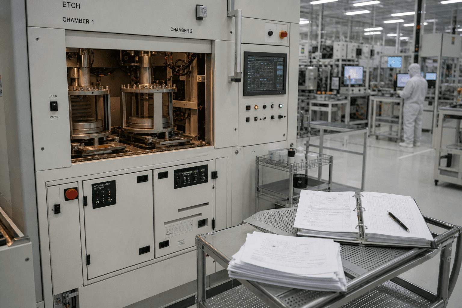
DOE report ET-09: the split-lot that blamed etch pressure and proved something else
Factor tables, wafer maps, and confirmation lots decide whether a process change is causal—semiconductor experiment report, not ion-implant dose chains, not wet-bath notebooks, not High-NA stitching programs.
29 Jul 2026

Semiconductors
Travelogue of FOUP #A-7741: contamination is a route, not a particle myth
Carrier history, AMHS handoffs, and loadport discipline decide whether wafers inherit foreign particles—semiconductor logistics-contamination story, not AMC detective timelines, not UPW purity loops, not photoresist track cold chain.
28 Jul 2026
Semiconductors
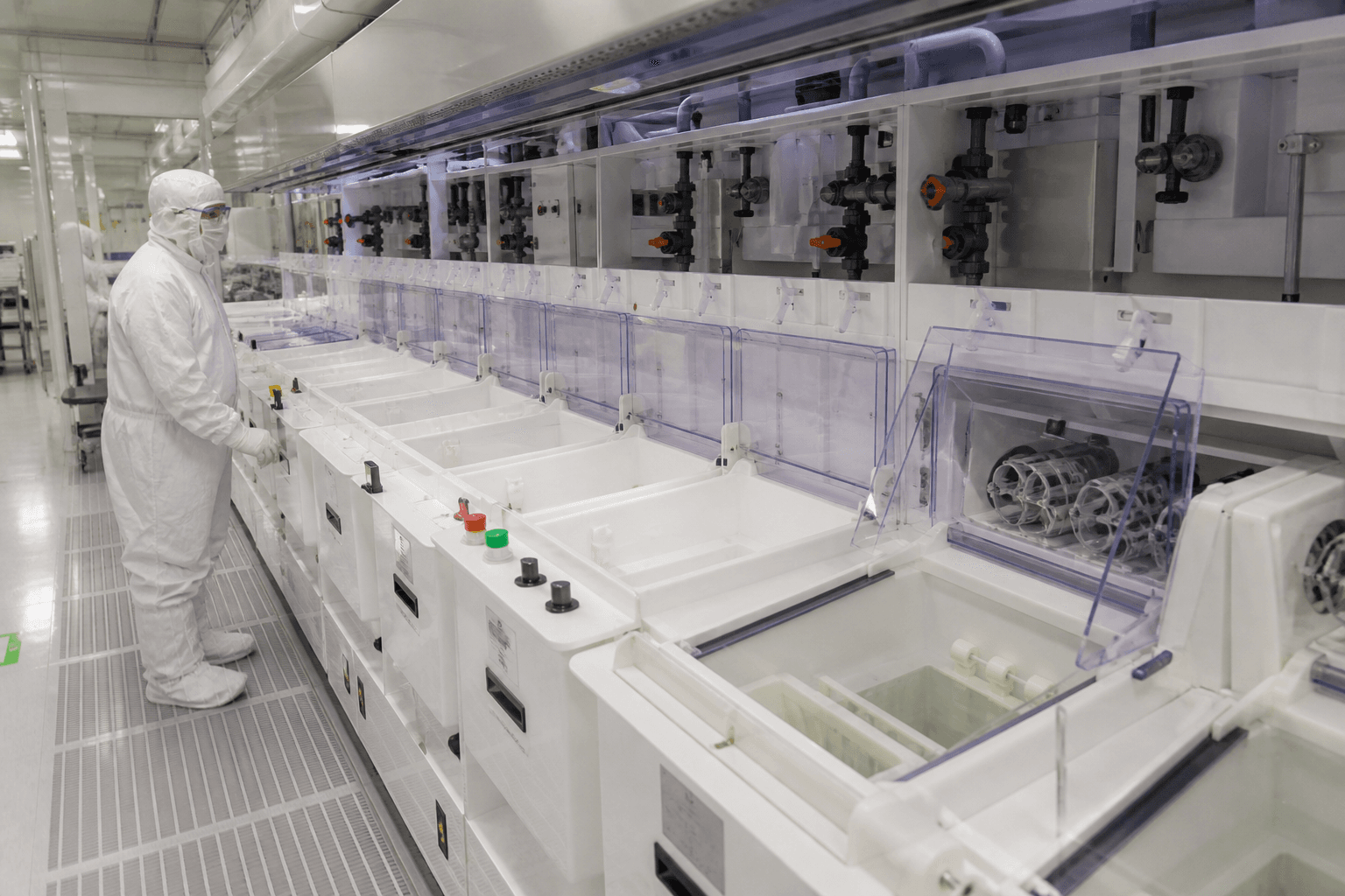
Lab notebook: wet-bench bath #7 and the lifetime nobody logged
Bath age, spike chemistry, and changeout triggers decide particle and etch drift—semiconductor wet-process notebook, not UPW loop purity, not CDA dew point, not photoresist track logistics.
28 Jul 2026
Semiconductors
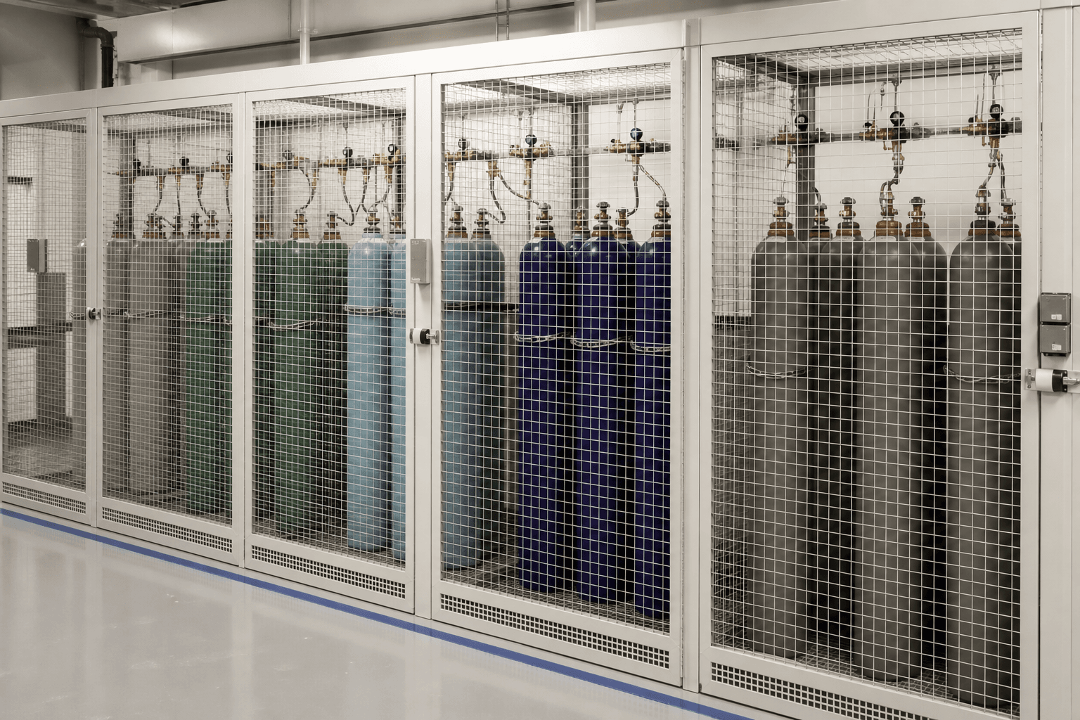
War-room transcript: neon, helium, and the fab that thought gas was a PO
Cylinder allocation, purity grades, and dual-source lies decide litho and etch uptime when specialty gases tighten—semiconductor materials capacity story, not photoresist cold chain, not CMP slurry totes, not dry-vacuum pump rebuilds.
28 Jul 2026
Semiconductors
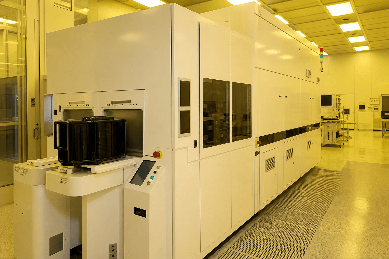
Follow the dose: ion implant as a closed measurement chain
Beam current, Faraday cups, charge neutralization, and dose SPC decide device parametric health—semiconductor metrology-control story, not photoresist track logistics, not High-NA stitching, not dry-vacuum pump reliability.
27 Jul 2026
Semiconductors
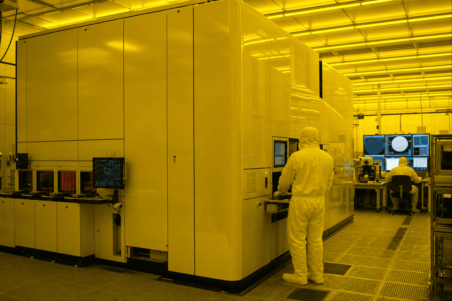
High-NA EUV fails as stitching and depth-of-focus, not as a scanner brochure
Field stitching, thin-resist DOF, and mask–etch co-optimization decide High-NA yield windows—semiconductor process story, not High-NA tool overviews, not pellicle logistics, not photoresist track cold chain.
25 Jul 2026
Semiconductors
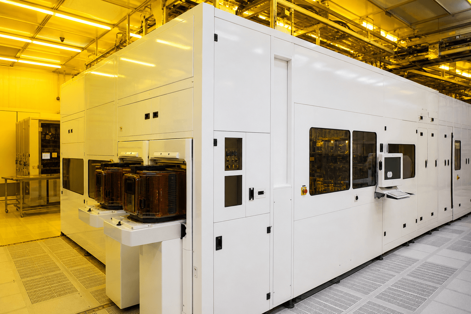
The track coater is a supply chain: when resist logistics fail, litho waits
Photoresist cold chain, dispense health, and coat uniformity decide lithography queue time—semiconductor consumables story, not EUV pellicle supply, not AMC hunts, not dry vacuum pumps.
24 Jul 2026

Semiconductors
The dry-pump war room: when tool vacuum becomes a fab capacity constraint
Dry vacuum pumps, forelines, and abatement decide etch/CVD uptime—semiconductor utilities story, not CMP slurry totes, not AMC hunts, not nitrogen blanketing.
23 Jul 2026
Semiconductors
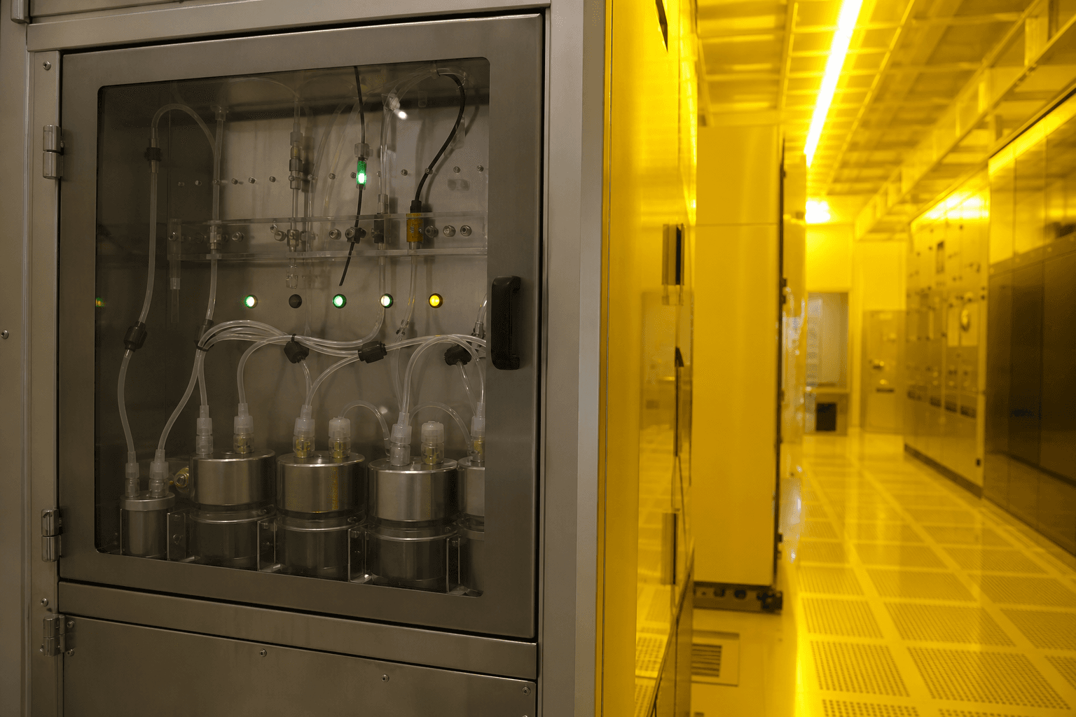
Hour 0 to week 2: how an AMC hunt actually clears a lithography bay
Airborne molecular contamination is a detective timeline for resists and optics—not CMP slurry logistics, not EUV pellicle supply, not cleanroom HVAC brochure math.
22 Jul 2026

Semiconductors
CMP slurry is a process chemical supply chain wearing a tote label
Particle size, pad pairing, and dual-source logistics decide polish yield—procurement timeline for fabs, not another substrate or mask story.
21 Jul 2026
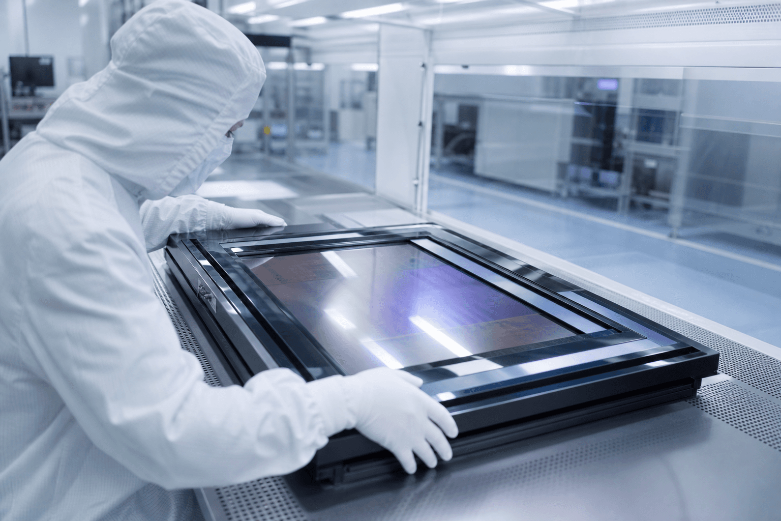
Semiconductors
EUV photomask and pellicle supply becomes the hidden lithography gate
Mask-shop capacity and pellicle yield own scanner utilization after the tool is installed—adjacent to High-NA CapEx and ABF substrates, focused on reticle logistics.
21 Jul 2026
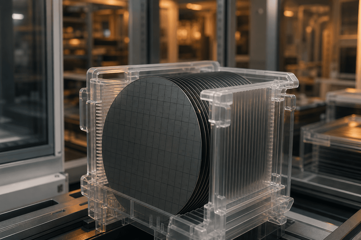
Semiconductors
SiC wafer supply becomes the bottleneck behind power device ramps
Boule-to-wafer capacity, defect density, and diameter transitions—distinct from SiC/GaN device headlines, SST racks, and industrial drive installs.
20 Jul 2026
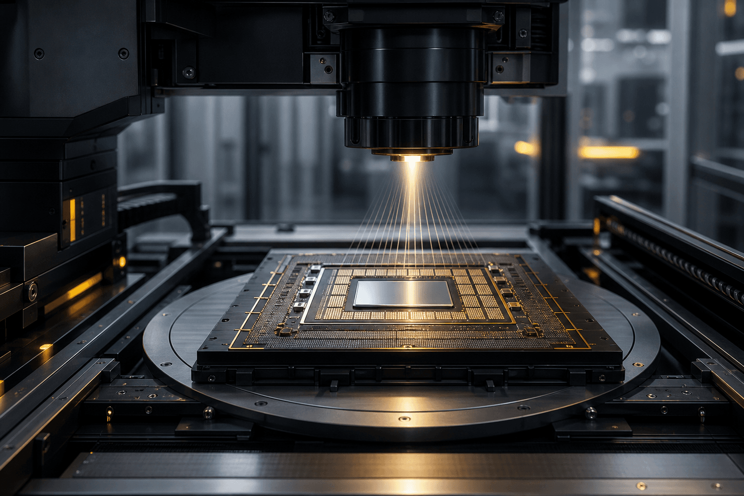
Semiconductors
Substrate warpage metrology becomes the quiet gate for large AI packages
Flatness measurement and process control on big organic and panel carriers—distinct from ABF capacity headlines, glass-core bets, and package test floors.
20 Jul 2026
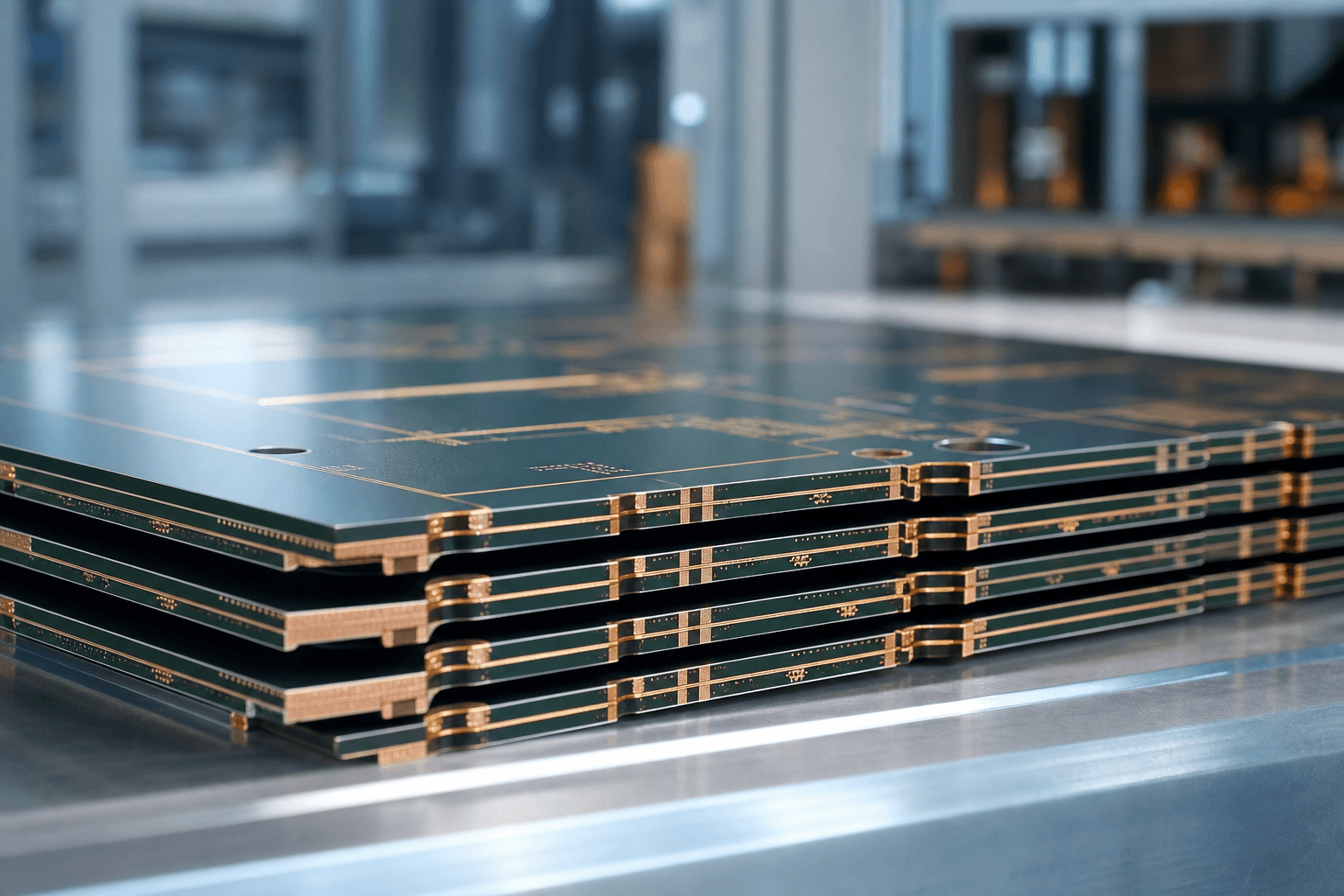
Semiconductors
ABF organic substrates remain the volume gate while glass pilots
Build-up ABF capacity and yield still ship most AI packages—distinct from glass-core bets, CoWoS/CoPoS lines, and package test floors.
19 Jul 2026
Semiconductors
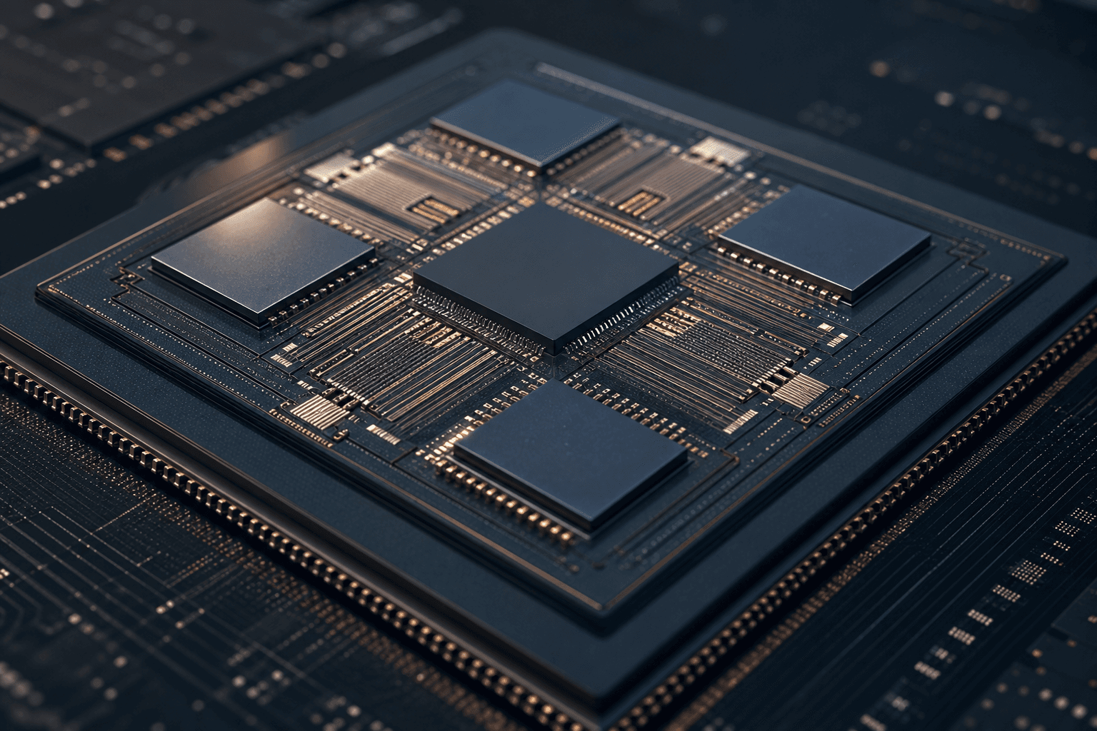
UCIe turns chiplet interconnect from slideware into a packaging contract
Die-to-die standard compliance and PHY constraints—distinct from chiplet export narratives, CXL pooling, hybrid bond yield, and CPO/LPO optics.
19 Jul 2026

Semiconductors
Package test and burn-in become the AI packaging throughput gate
Handler, socket, and burn-in capacity now limit advanced AI packages—downstream of CoWoS, hybrid bond, and glass substrates.
17 Jul 2026
Semiconductors
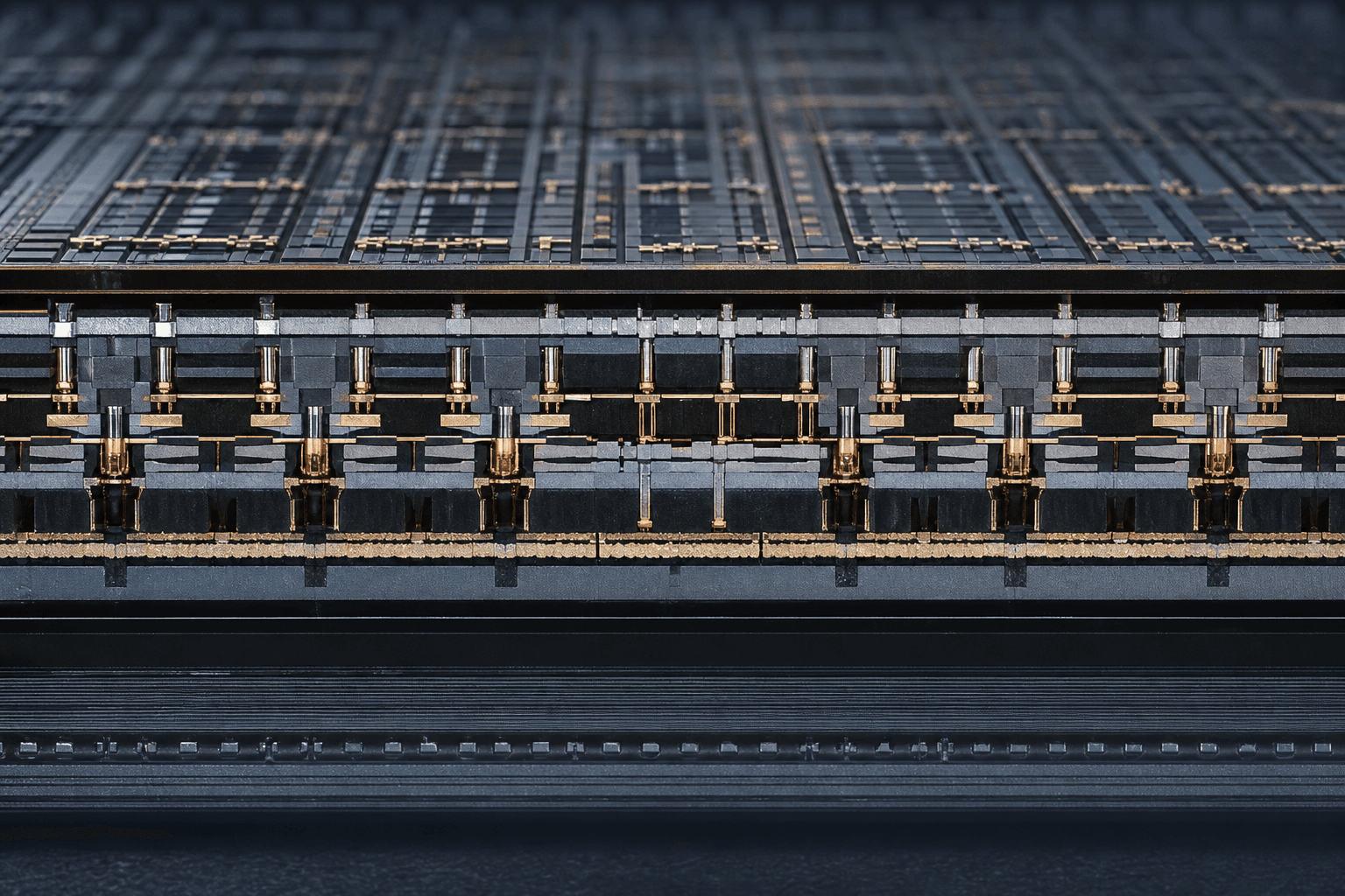
CFET stacking becomes the density bet after nanosheet GAA
Complementary FET vertical stacking targets continued logic shrink—distinct from GAA risk ramps, hybrid-bonded HBM, and advanced packaging races.
11 Jul 2026
Semiconductors
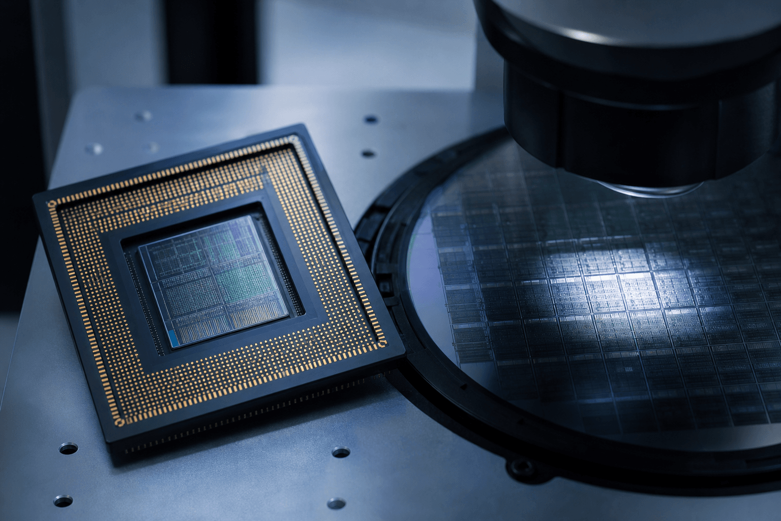
Processing-in-memory targets AI’s data-movement tax
PIM and near-memory compute aim to cut HBM shuttle energy for inference and embedding workloads—architecture relief, not another packaging or bonding race.
06 Jul 2026
Semiconductors
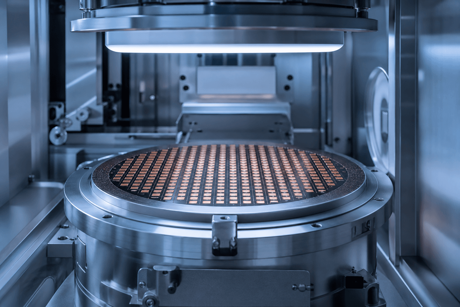
Hybrid bonding becomes the yield gate for AI HBM stacks
Cu-Cu and hybrid bonding move HBM and logic closer—capacity follows bond yield and cleanroom CapEx, not only wafer starts or substrate roadmaps.
01 Jul 2026
Semiconductors
Glass-core substrates become the next AI packaging materials race
Through-glass vias and glass cores are leaving the lab—pilot lines and JVs target 2026–27 qualification as organic substrates hit warpage and size limits on large AI packages.
28 Jun 2026

Semiconductors
GAA nanosheet logic moves from roadmap slide to risk production
Gate-all-around transistors are no longer a future node promise—18A-class flows with RibbonFET-style devices are in risk production, pairing GAA with backside power for AI-era density.
24 Jun 2026

Semiconductors
LPO optics bridge AI fabrics before full CPO lands
Linear and other pluggable optical paths are taking 2026 volume while co-packaged optics mature—lower power than copper, less integration risk than CPO, and a real procurement choice for scale-out.
19 Jun 2026

Semiconductors
CXL memory pooling becomes AI’s capacity bypass
When HBM and GPU packages hit cost and supply walls, CXL fabrics let racks share commodity DRAM—slower than HBM, but cheaper capacity that stops buying compute just to get memory.
14 Jun 2026

Semiconductors
Chiplets and 3D stacking become the export-control workaround
With advanced EUV access constrained, designers push performance through packaging—chiplets, hybrid bonding, and vertical stacks—turning architecture into a geopolitics strategy.
09 Jun 2026
Semiconductors
HBM4 turns memory into the AI supply-chain race
Mass production and early HBM4E samples in 2026 reset who can feed the next accelerator wave—base-die process, stack height, and customer qualification now matter as much as DRAM bits.
04 Jun 2026

Semiconductors
Backside power delivery becomes an AI-node design constraint
Routing power from the wafer backside frees front-side interconnect for signals—but process complexity, thermal paths, and yield learning decide who ships it first.
30 May 2026

Semiconductors
High-NA EUV becomes a fab CapEx and process decision
0.55-NA EUV tools are entering qualification for sub-2nm work—but cost, throughput, and whether multipatterning on 0.33-NA still wins remain the real roadmap questions.
25 May 2026

Semiconductors
Co-packaged optics moves from demo to AI fabric constraint
As switch ASICs and GPU clusters push past copper limits, CPO promises lower energy per bit—while yield, lasers, thermal design, and serviceability decide real adoption.
23 May 2026
Semiconductors
From CoWoS to CoPoS: panel packaging enters the AI roadmap
Wafer-level advanced packaging is still the workhorse, but panel-level platforms are being qualified to stretch size, cost, and throughput for the next wave of accelerators.
21 May 2026
Semiconductors
Advanced packaging and HBM now set the AI chip pace
Leading-edge wafers are only half the story. CoWoS-class packaging and high-bandwidth memory allocation decide which AI accelerators reach volume.
19 May 2026