
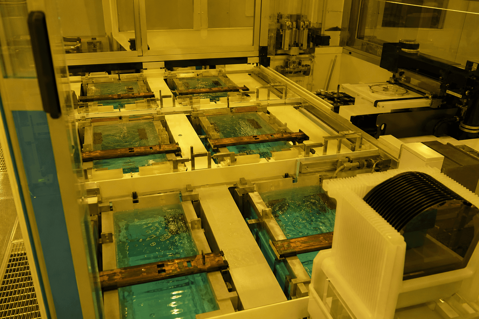
Damascene and advanced interconnect flows treat electrochemical deposition (ECD) as a capacity asset: wafers in, copper out, green light. Yield meetings then discover edge-thick rings, center starve, or feature-scale fill voids that look like “CMP overpolish” or “etch bias” two modules later. The plating bay was never asked to prove uniformity as a controlled output—only that the robot finished the recipe.
CMP pad and conditioner briefs own planarization consumables. Wet-bench titration owns etch/clean baths. Photoresist track owns coat logistics. This brief owns copper ECD bath and electrical honesty as the gate before those downstream excuses.
What the green lamp cannot prove
Additive package state. Accelerators, suppressors, and levelers deplete and break down on different clocks. A weekly “chemistry OK” sticker that ignores CVS (or equivalent) trends is folklore. Blind top-ups invent transient fill windows that scrap fine features.
Anode and contact integrity. Consumed anodes, filmed contacts, and uneven wafer clamp contact change local current density while the power supply still reports the commanded amps. The recipe ran. The map did not.
Flow and mass transport. Recirculation rate, filter differential pressure, and agitation that died on one quadrant produce thickness and void signatures that look random until someone overlays the flow schematic on the metrology heatmap.
Feature-scale vs wafer-scale. Superfill that works on the coupon may still leave a wafer-edge exclusion that eats scribe and edge-die yield. SPC that only watches mean thickness hides the radial slope that kills the next module.

Control loop that fabs actually run
| Signal | Why it is first-class | Typical failure if ignored | |--------|------------------------|----------------------------| | Additive assay / CVS trend | Separates depletion from contamination | Sudden fill voids after “normal” top-up | | Bath metal & acid balance | Sets plating rate envelope | Drift blamed on rectifier | | Anode mass / contact resistance | Protects current distribution | Edge-thick maps after anode change | | Recirc ΔP & flow | Confirms mass transport | Quadrant starve with green tool state | | Within-wafer thickness map SPC | Catches slope before CMP excuses | Overpolish scrap two tools later | | MoC on recipe + chemistry + hardware | Keeps genealogy honest | “Same recipe” after three silent changes |
Disposition discipline
Do not disposition a thick edge as “CMP will take it” without a written budget against the CMP process window. Do not release a bath after a large additive spike without a short monitor-wafer campaign. Do not treat plating current as a constant when contact resistance trends are open tickets.
An anonymized logic fab spent two weeks chasing CMP pad life after edge-thick copper maps appeared on three ECD chambers. Pads were fine. One chamber had a partially filmed anode set and a filter near bypass; mean thickness SPC stayed inside limits while radial range doubled. The fix was anode and filtration MoC—not a new conditioner SKU.
Boundaries
Specialty-gas neon/helium stories own cylinder logistics. ESC helium owns chuck cooling leaks. Chamber seasoning owns first-wafer effects after wet cleans. This page owns ECD copper as a thickness-and-fill process, not as a throughput lamp.
If the next module’s scrap map looks like a plating radial, believe the map. Ask the bath and the current path before you rewrite the CMP recipe.