
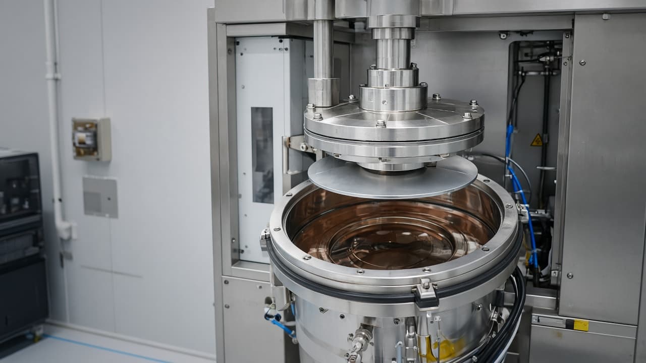
Copper ECD process windows are argued as current density, additives, and bath age. Those matter. The wafer that enters the plating cell already carries a seed layer that decides whether current can start uniformly. Thin seed, discontinuous seed, or edge-thin maps produce voids, roughness, and within-wafer thickness ranges that look like “plating tool drift” on the scrap ticket.
Copper ECD plating uniformity and CMP dishing own later steps. Barrier/liner integrity is adjacent. This page is copper seed layer continuity and thickness as the ECD entry condition.
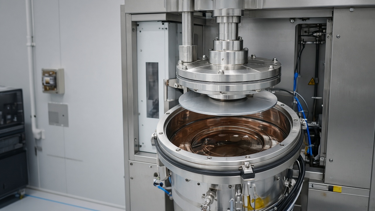
Seed is typically a thin copper film (often on a barrier) deposited so the electrolyte can drive nucleation everywhere the feature needs metal. Where seed is missing or too resistive, plating starts late or not at all—voids at the bottoms of vias and trenches follow. Over-thick seed eats into the fill budget and can worsen topography after polish. Track seed thickness mean and range after PVD/CVD chamber events, target changes, and long idle periods that oxidize the surface before plate.
Disposition habits that save the ECD cell
Hold lots against seed metrology when ECD thickness or void maps shift without a bath change. Re-qualify seed chambers after PM with monitors that include edge sites, not only center. Do not “fix” ECD by raising current to overcome a starved seed—that usually trades one defect mode for another.

Bath chemists can tune additives for weeks. They cannot invent conductivity where the seed never landed. Sites that trend seed with ECD genealogy stop rewriting plating recipes for a deposition problem two tools upstream.