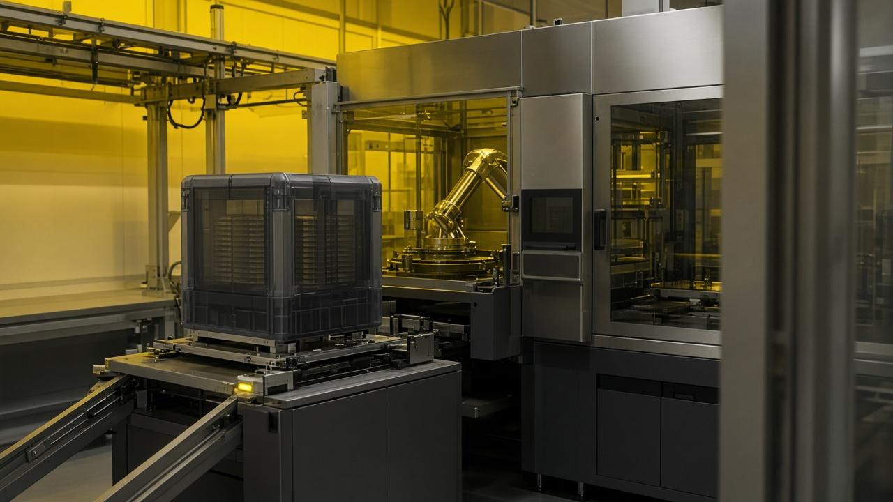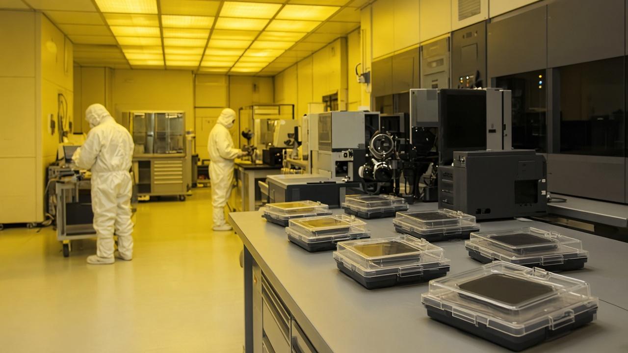
On 8 September ASML and TSMC announced a collaborative industry initiative, formed the day before ahead of SPIE BACUS in Monterey, to drive the semiconductor supply chain toward 12-inch EUV photomasks for High NA lithography. The stated waypoints are a 12-inch mask pilot line by 2031 and full lithography-system readiness for advanced-node production by 2033. Near-term High NA production remains on today’s 6-inch mask format; the larger blank is framed as the later productivity step that lifts scanner throughput and eases stitching limits.
TSMC said it intends to use ASML High NA in high-volume manufacturing for advanced nodes starting in 2030, with High NA layer count expected to rise as transistor stacks for AI workloads grow more complex. ASML CEO Christophe Fouquet positioned 12-inch masks as the follow-on that raises scanner productivity once High NA adoption deepens. The release notes that other High NA adopters and major suppliers expressed interest in joining; it does not publish a membership roster or binding supply contracts.
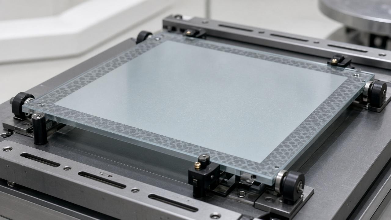
An industry initiative with 2031/2033 milestones is not a 12-inch mask line running today, not a scanner SKU shipping for 12-inch reticles in 2026, and not a rewrite of Intel’s or others’ current 6-inch High NA HVM paths. What the September note actually locks is the ASML–TSMC collaboration, the pilot and production target years, and the statement that near-term High NA stays on 6-inch masks until the larger format is ready.