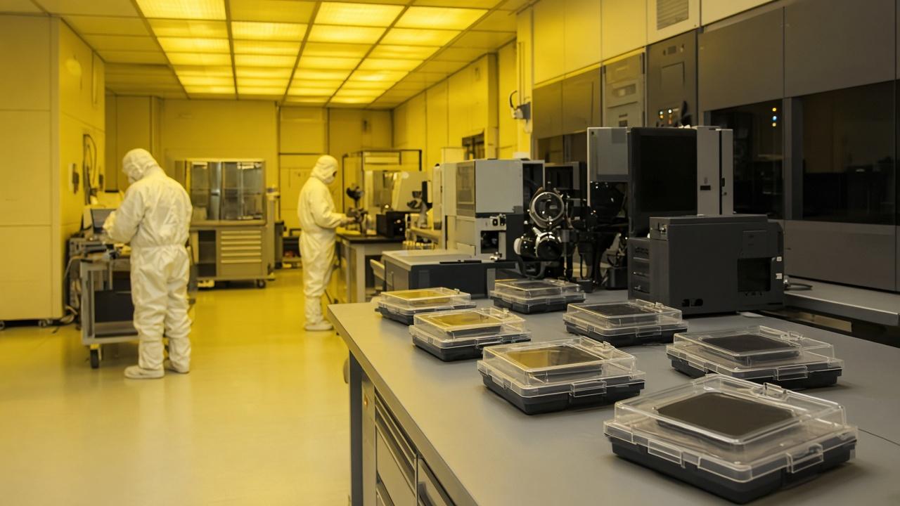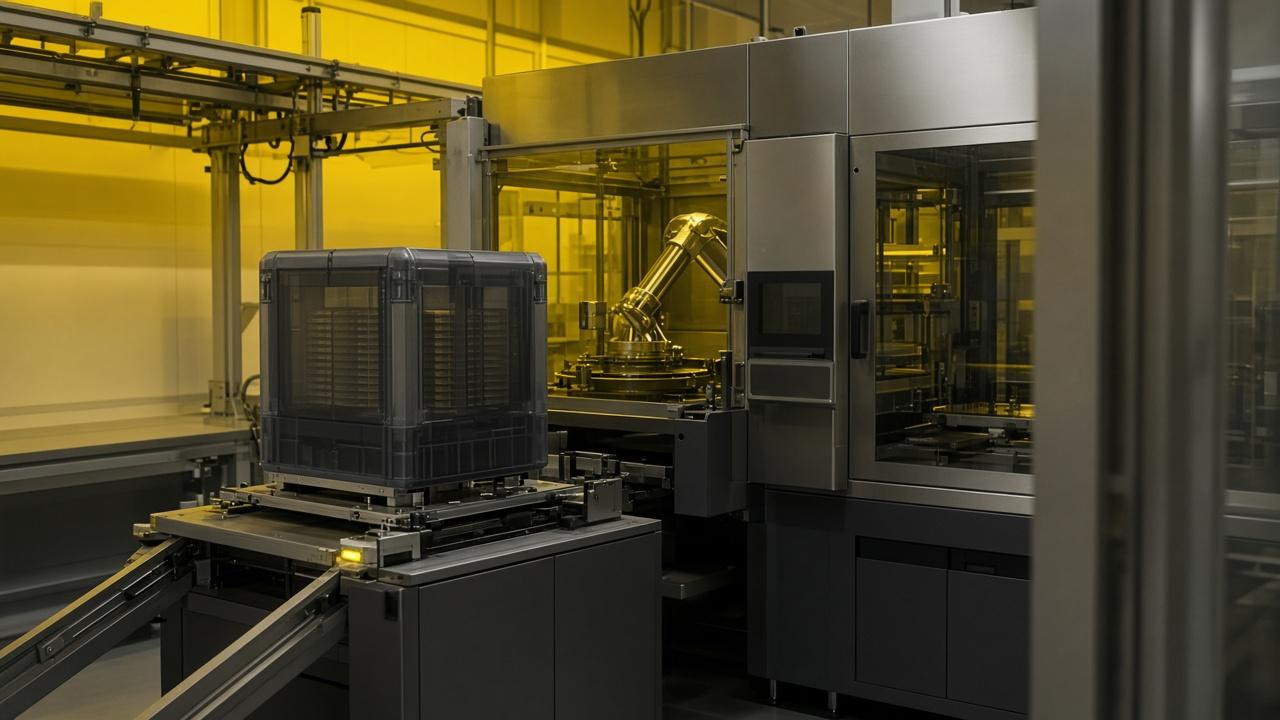
Infineon Technologies said on 9 November that it has successfully processed 300-millimeter silicon carbide wafers into functional power devices at its fab in Villach, Austria. The company positions the result as the first of its kind in a full-scale semiconductor fab environment and says the work used existing silicon manufacturing equipment. Infineon plans to show a processed 300 mm SiC wafer at electronica in Munich from 10 to 13 November.
Chip count on 300 mm versus 200 mm is stated as 2.3 times more devices per wafer—Infineon’s area comparison. The firm says the milestone demonstrates potential for later full-scale industrialization of SiC on 300 mm, while 300 mm technology and ramp timing will be planned with customers and partners and the 200 mm SiC manufacturing roadmap continues. Target markets named in the release include automotive, renewable energy, industrial, and AI data-center power conversion under the CoolSiC portfolio. A separate Cold Split feasibility note at Dresden is a boule-separation materials step, not the Villach device result.
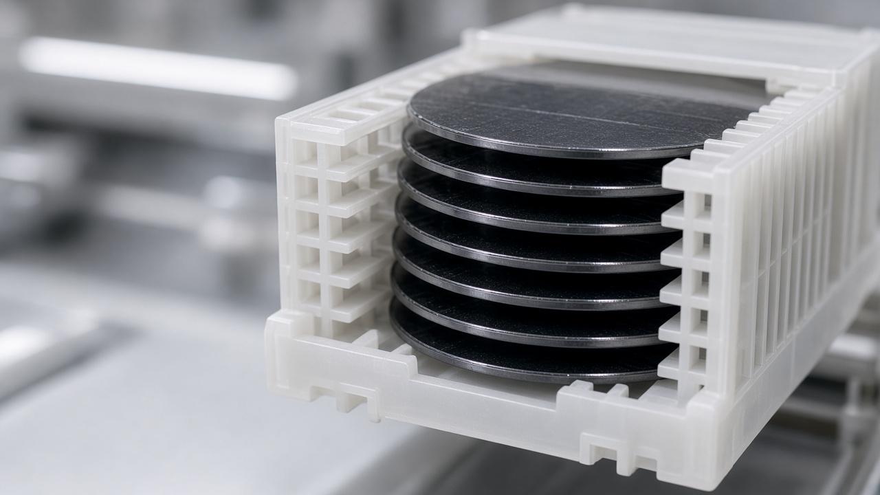
Functional devices mean Infineon measured working power parts from the 300 mm flow. That is feasibility, not a published yield, not a qualified PDK for external foundry sale, and not a date when 300 mm SiC replaces 200 mm supply. Keep Villach, the existing-tool claim, the 2.3× chip-count statement as Infineon’s figure, and the explicit continuation of the 200 mm roadmap.