
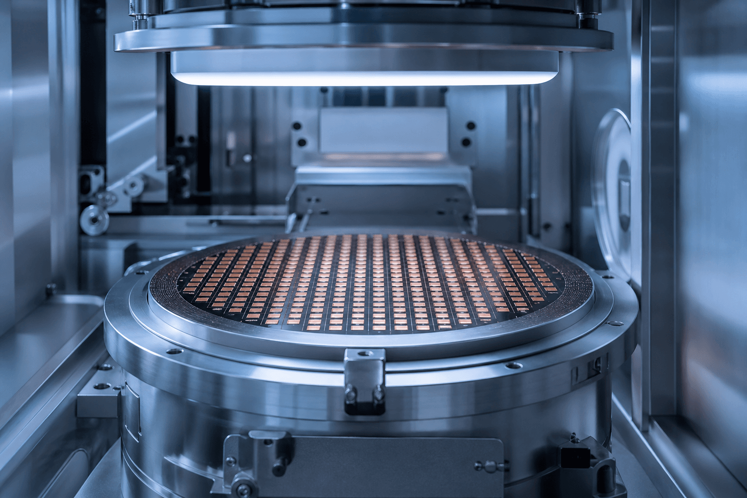
HBM supply races and glass-core substrates grab headlines. The quieter gate for next-generation stacks is hybrid bonding: copper-to-copper joins that replace or shrink solder bumps so dies can sit denser and cooler. Logic-on-memory and memory-on-memory flows now treat bond alignment, surface prep, and defectivity as capacity limiters equal to the DRAM or logic wafer.
The industrial point is packaging physics as a fab constraint. You cannot schedule AI accelerators on bond tools that scrap stacks at the last step.
What hybrid bonding changes
- Interconnect density — Finer pitches than microbumps for bandwidth and power.
- Stack height — Thinner joins that matter for thermal and package z-height.
- Tooling CapEx — Dedicated bonders, metrology, and clean handling become bottlenecks.
What still hurts
Particle and oxide control dominate yield more than slideware pitches. Rework is limited; a bad bond kills an expensive multi-die stack. Roadmaps that ignore bond learning curves over-promise HBM4-class volume. This is not CoPoS panel politics, not backside power delivery, and not LPO/CPO optics—those sit elsewhere in the AI build.
What to watch next
- Which OSATs and IDMs publish stable hybrid-bond yields at AI stack volumes.
- Whether bond metrology becomes a gated step in customer qualification.
- CapEx lead times for bonders versus HBM wafer supply as the binding constraint.
Glass cores reshape the substrate. Hybrid bonding decides whether the stack survives assembly.