
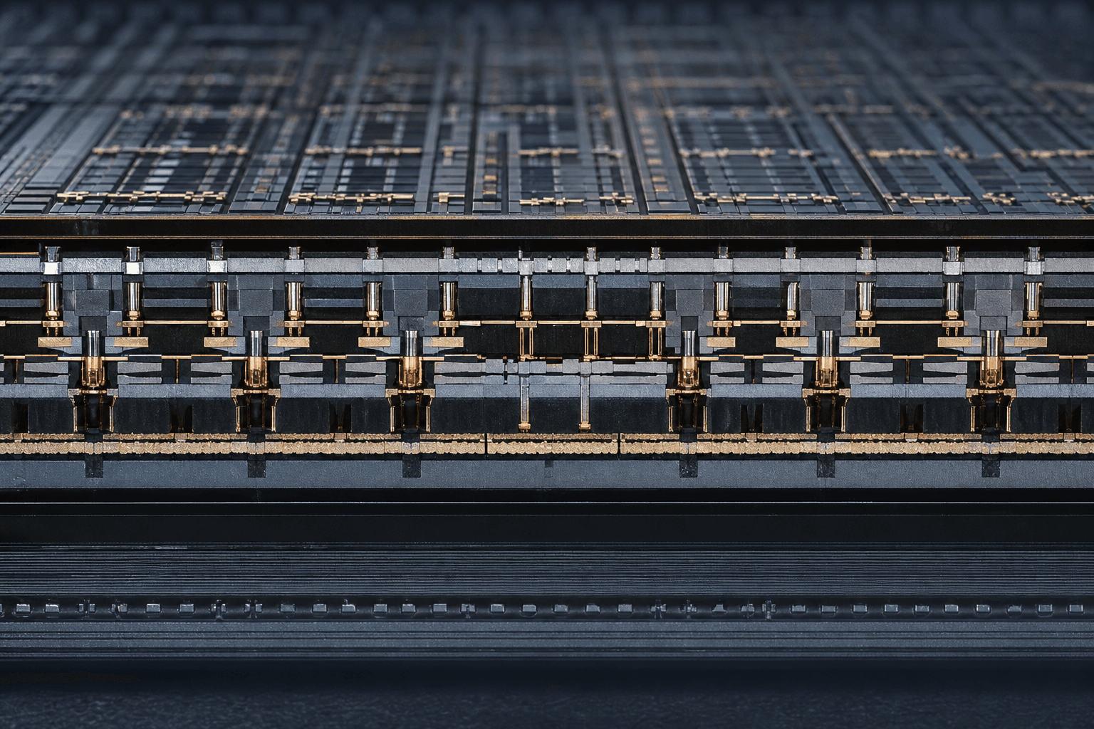
GAA nanosheets are entering risk production. Hybrid bonding and HBM dominate packaging narratives. The next transistor density story is complementary FET (CFET): n- and p-channel devices stacked vertically to reclaim footprint after planar and FinFET levers are exhausted.
Foundries and tool vendors are aligning CFET process modules—selective epitaxy, middle-dielectric isolation, and tight contact overlays—toward late-decade logic nodes rather than slideware.
The industrial point is CapEx and yield for stacked logic, not another packaging acronym.
What CFET changes
- Footprint recovery — Vertical n/p stacking where GAA alone plateaus.
- Tooling roadmaps — Epitaxy, etch, and metrology tuned for stacked complementary channels.
- Design rules — PDK timing for when CFET is more than a paper node.
What still fails
Confusing CFET with 3D NAND-style stacking or chiplet packaging. Betting on volume dates before contact resistance and thermal paths are credible. This is not hybrid bonding for HBM, not backside power delivery alone, and not High-NA EUV as the sole bottleneck story.
What to watch next
- Which foundries publish CFET pilot yield windows, not only cross-sections.
- EDA readiness for stacked complementary parasitics.
- Whether CFET slips as GAA learning curves consume the CapEx budget.
GAA is the current climb. CFET is the next wall after the ridge.