
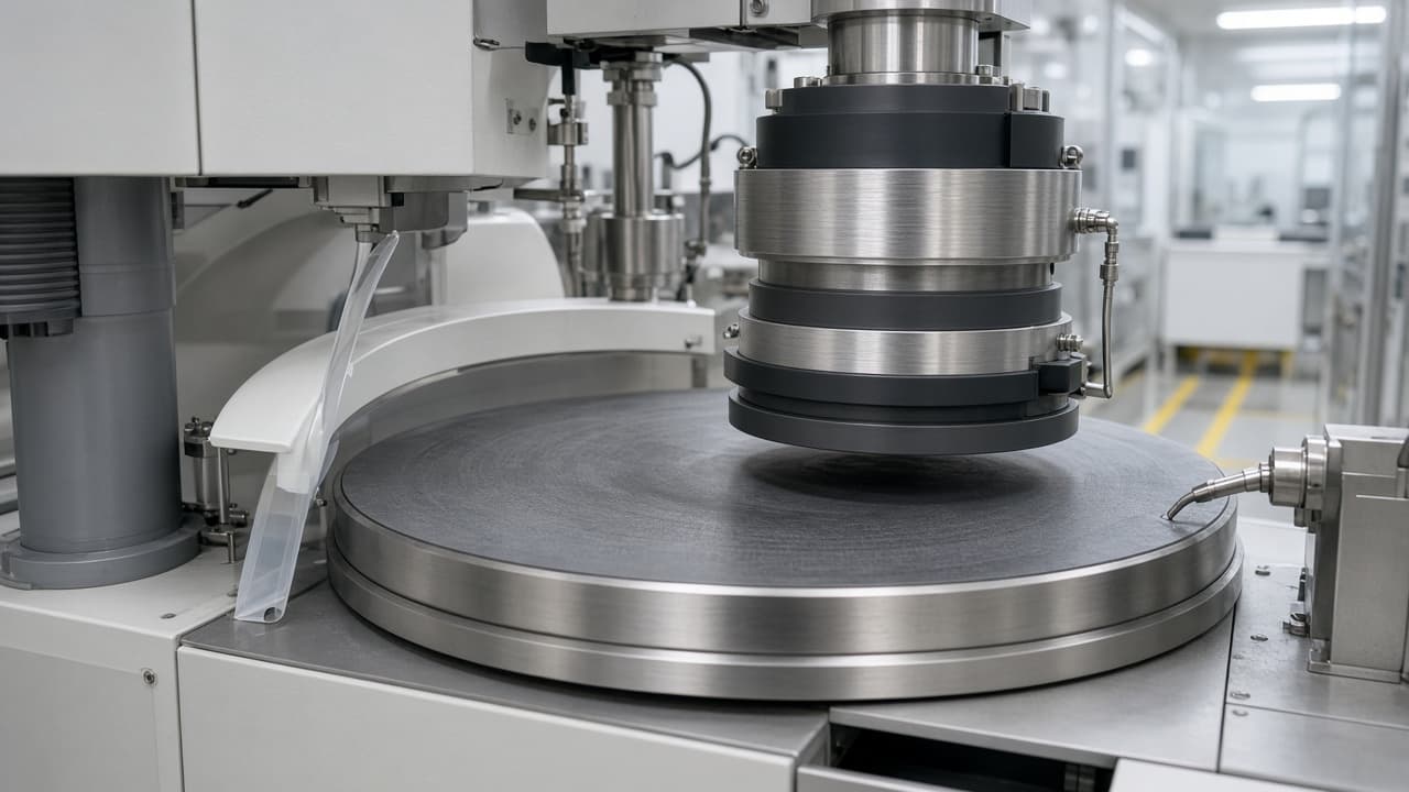
Copper chemical-mechanical planarization is sold as a thickness and residual-metal story. On the floor it is often a topography story. Wide lines dish. Dense arrays erode. The wafer leaves the polisher “clear” on an optical endpoint and still carries enough relief to wreck depth of focus two modules later.
CMP slurry supply, pad conditioner life, and chamber matching are neighboring tickets. This page is copper CMP dishing and erosion as process control—pattern-density effects, overpolish budget, and metrology that actually maps the relief.
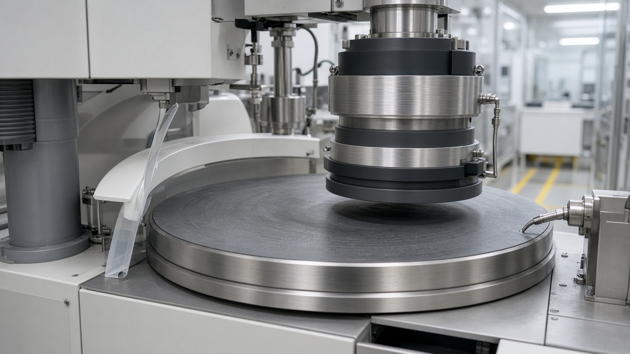
Dishing is preferential removal of soft copper in wide features relative to surrounding dielectric or barrier. Erosion is thinning of the dielectric stack in dense patterned regions when polish continues after copper clears. Both grow when:
- Endpoint is late or noisy, so the recipe leans on a fixed overpolish time sized for the worst die.
- Slurry selectivity drifts after a lot or temperature change.
- Pad glaze or conditioner under-dressing changes contact mechanics across the wafer.
- Pattern density on a new tape-out was never represented on the monitor wafers used to set the polish window.
Metrology that belongs in the disposition
A single center-site copper thickness does not own dishing. Profilometry or high-resolution thickness maps on representative wide and dense structures do. Trend dishing depth and erosion against polish time, conditioner counts, and slurry lot. When lithography focus budgets shrink, pull the last CMP topography lot genealogy before you rewrite the scanner recipe.
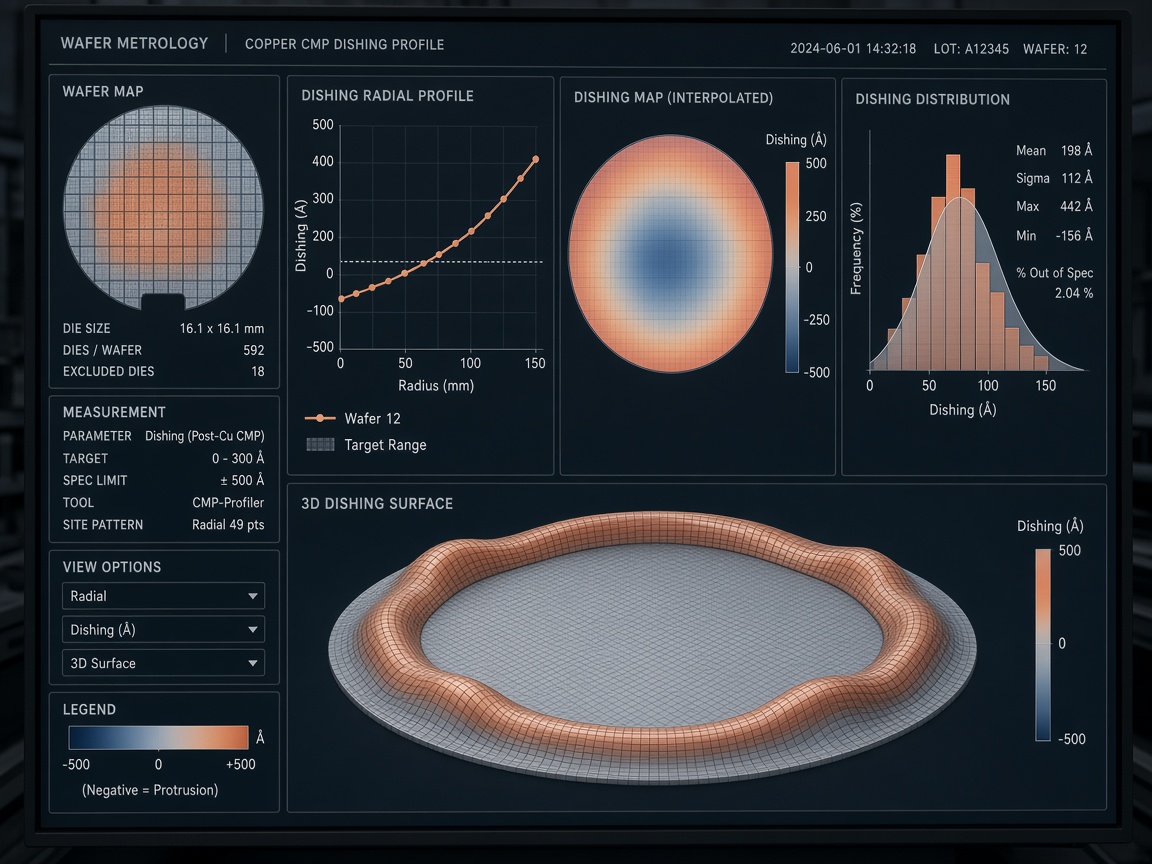
Clearing residual copper matters. So does stopping before the polish invents a new topography specification the rest of the line never agreed to. Sites that only watch “Cu clear” lamps fund quiet yield loss at the next patterning step.