
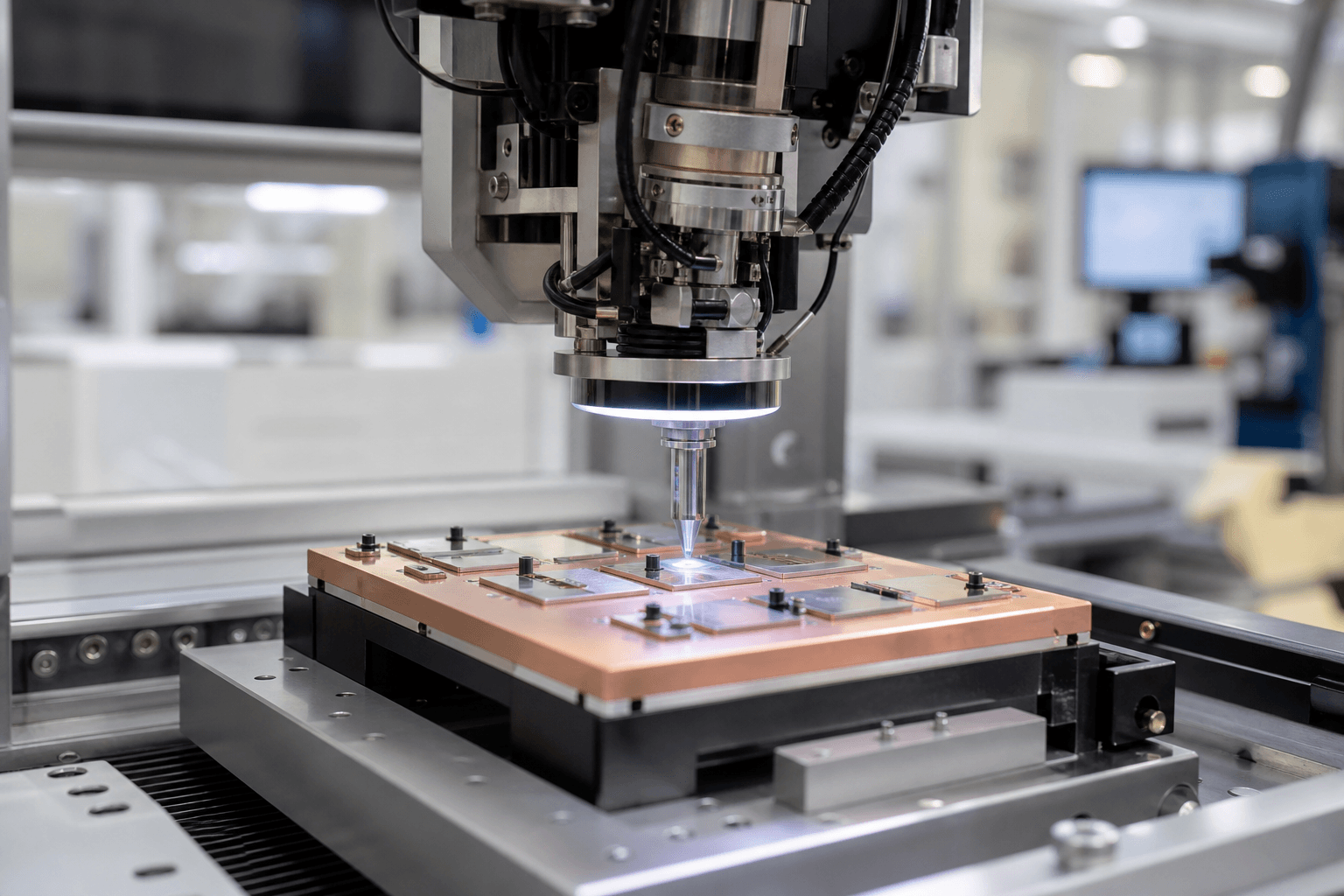
Power modules for traction inverters, AI power shelves, and industrial drives push heat through die attach long before plastic packaging aesthetics matter. Soft solder hit limits. Silver sinter (and related sinter die-attach systems) promise lower thermal resistance and higher temperature duty—if bond-line thickness, porosity, and process pressure are real capabilities, not brochure photos.
Hybrid bonding owns HBM interfaces. Molded underfill owns polymer voids on large AI packages. Package burn-in owns outgoing screens. This brief owns die attach as the thermal joint between silicon and the rest of the world.
What sinter process control actually watches
- Paste / preform genealogy — lot, age, storage humidity.
- Dispense or place uniformity — bond-line thickness windows.
- Pressure and temperature profiles — sinter densification, not “oven recipe folklore.”
- Void / porosity metrology — sampling that can stop a lot.
- Post-attach shear / thermal resistance correlation — on golden modules, not only visual shine.
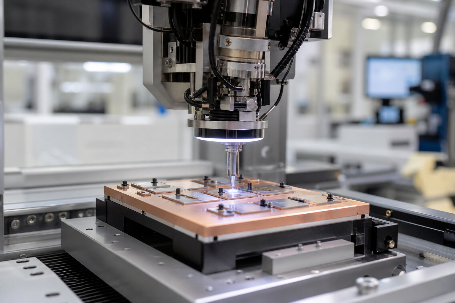
A shiny fillet story does not equal a low-void sinter joint.
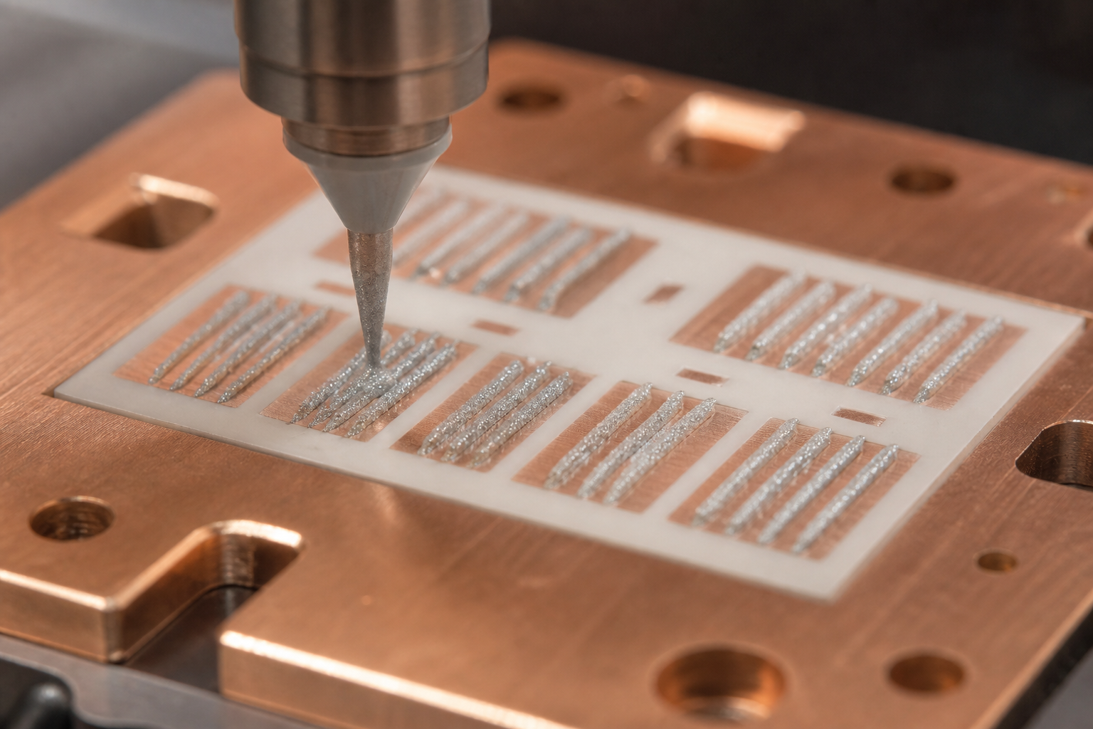
Coat weight and pattern are thermal parameters.
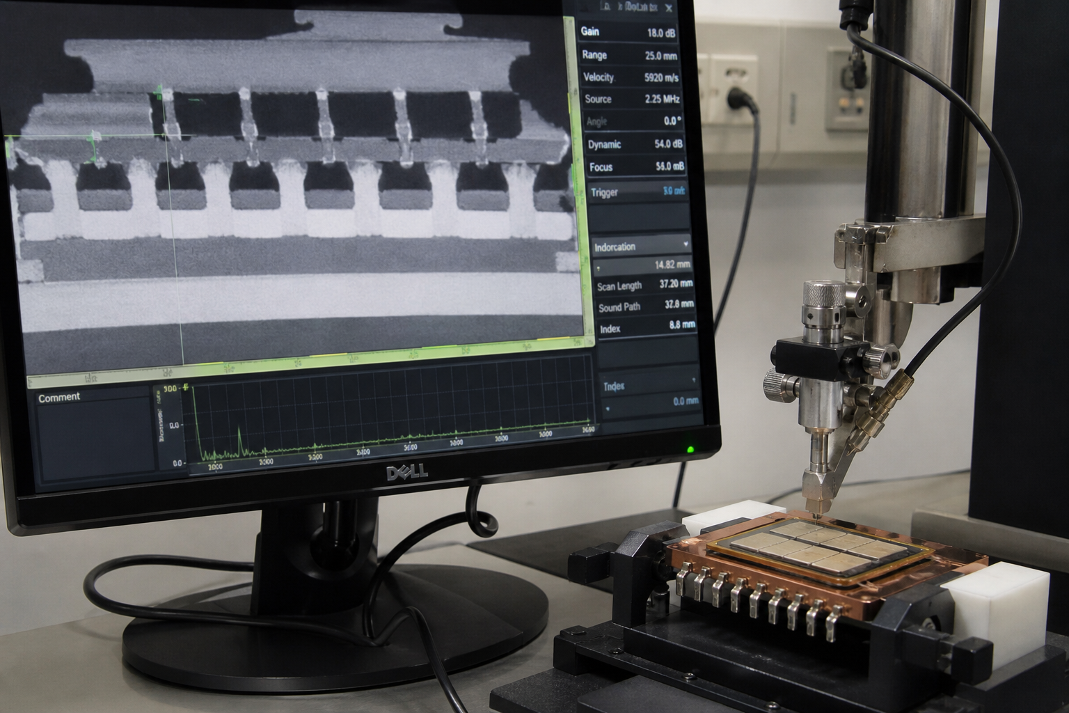
If voids cannot hold a lot, inspection is theater.
Why power packaging feels this first
SiC and GaN shrink conduction losses and raise allowable junction temperatures—until the attach layer becomes the bottleneck. Modules that pass electrical test and fail thermal cycling often failed the joint, not the die datasheet. Plants that treat sinter like “just another epoxy die attach” inherit field returns dressed as “application abuse.”
Adjacent fences
SiC wafer/epi briefs own substrate and epitaxy. SiC/GaN device briefs own switching. Underfill voids own polymer fill on logic packages. Advanced package test owns screens. This page owns sinter die attach as power-module thermal integrity. Do not celebrate a wide-bandgap die and discover the bond line is a sponge.