
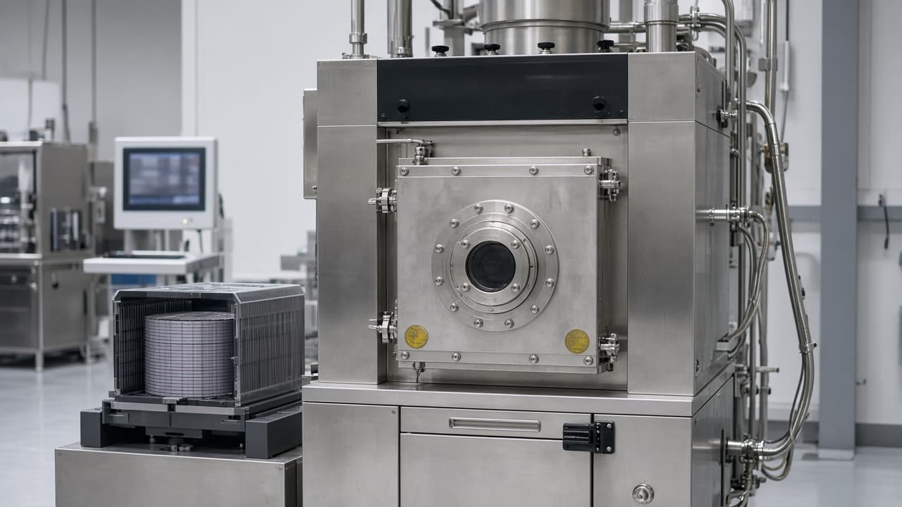
Most yield meetings argue about center-die maps. A surprising fraction of particle excursions, film peeling, and edge-die loss starts where the wafer is thinnest in process attention: the bevel and near-edge exclusion. Bevel etch (and related edge-clean / edge-bead removal steps on tracks) exists to remove unwanted film and residue from that rim so later modules do not redistribute it.
CMP pad life and copper ECD uniformity own planarization and plating. Temporary bonding owns thin-wafer handling. This article owns bevel and edge as a process module with its own recipe and scrap path.
Why the edge is not cosmetic
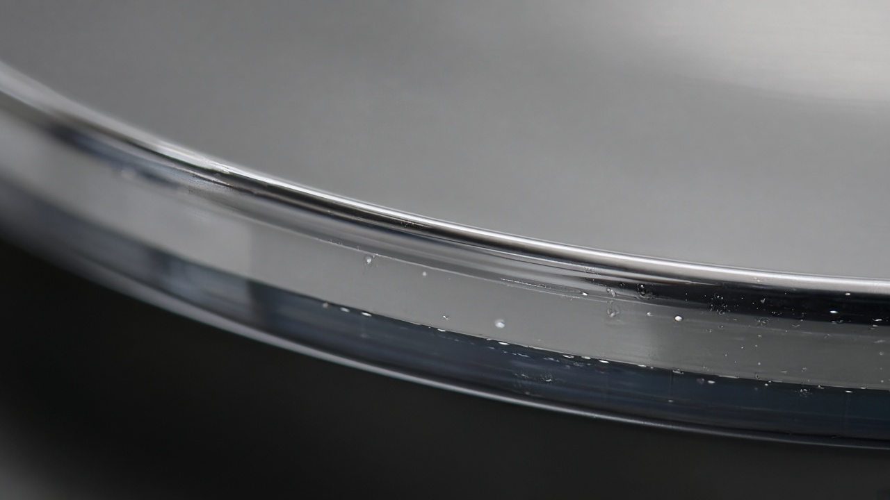
Clamps, pins, and FOUP contacts touch the periphery. Films that survive on the bevel flake into the next chamber or into the cassette. Edge exclusion that is too aggressive wastes die; exclusion that is too loose leaves residue that looks like a mysterious center defect two tools later. Bevel profiles also matter for bonding and grinding stacks where mechanical stress concentrates at the rim.
What to control
Recipe intent should name chemistry, time, and how far the etch or clean reaches into the frontside exclusion—not only “bevel on.” Monitor wafers and edge-inspection metrology belong in the same MoC as a chemistry change. Chamber matching on a bevel module is as real as matching on etch: kit age, electrode or lamp hours (depending on tool type), and season effects change edge maps even when the frontside recipe screenshot looks identical.
Ownership
If bevel is “owned by facilities” or “owned by whoever has time,” edge particles will keep arriving in other modules’ scrap codes. Name a process owner, a requal after wet cleans, and a rule for when edge-inspection fails block the lot versus trigger a tool inhibit.
The center of the wafer cannot stay clean if the rim is a particle factory. Treat bevel as process—or keep blaming the next tool for films that walked in from the edge.