
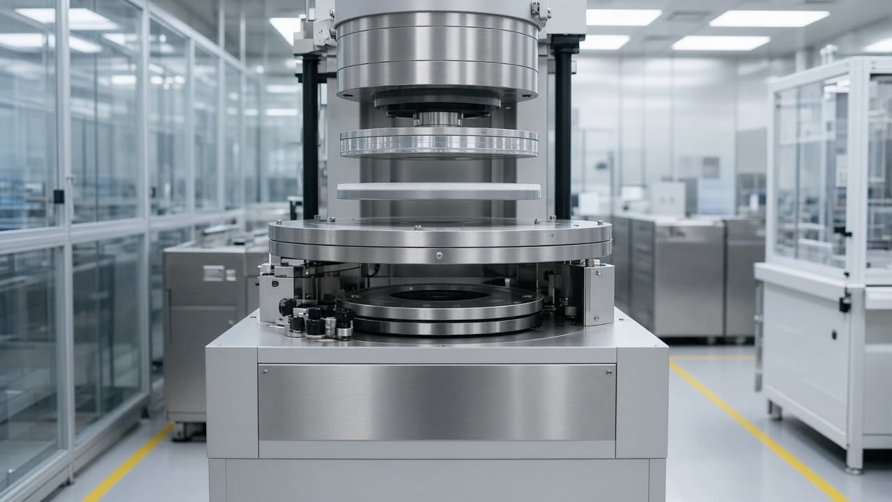
Advanced packaging and power-device flows often need wafers thinned far beyond what a free wafer can survive on standard handlers. Temporary bonding attaches the device wafer to a carrier so grinding, CMP, via formation, or backside metallization can proceed. Later, a thermal, laser, mechanical, or chemical release separates the pair. The bond step is not cosmetic. It is structural logistics for thin silicon.
Hybrid bonding and silver sinter die attach address permanent joins. This article is about temporary carrier bonding and debond as a process module with its own defect modes.
What must stay true through the stack
Bond uniformity matters because thin-wafer grinding and subsequent lithography or etch see the bonded pair as a mechanical system. Voids, particles, or thickness variation in the temporary adhesive or release layer translate into local stress, focus issues, or breakage. Carrier cleanliness and flatness are part of that system—not a facilities footnote.
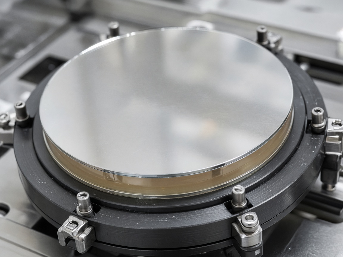
Debond is equally process-critical. Incomplete release leaves residue that contaminates downstream clean steps. Aggressive release that damages the device surface defeats the reason the carrier was used. OEM and materials suppliers publish different release chemistries and laser or thermal recipes; the fab window still belongs to that material set and tool family under MoC.
Practical control points
- Treat bond void and thickness metrology as release gates for thinning lots, not as optional engineering samples.
- Track carrier reuse cycles and clean status; a “known good” carrier with a scratched face is not known good.
- Correlate post-debond inspection (residue, crack, edge chip) with bond recipe and release method before changing grind parameters alone.
- Keep genealogy: device wafer ID, carrier ID, adhesive/release lot, bond tool, and debond tool on the same traveler.
Temporary bonding exists to make thin wafers handleable. If debond yield and cleanliness are not measured with the same seriousness as the grind recipe, the carrier is only postponing scrap.