

Advanced packaging roadmaps celebrate interconnect density: hybrid bonds, HBM stacks, large organic or glass-core substrates, panel dreams. Those slides can all be “green” while the package still dies in the field from something less glamorous—underfill that did not fill, cured around a void map that acoustic microscopy only found after a customer returned a board.
Capillary underfill and molded underfill (MUF) are not cosmetics around a chip. They are the mechanical and moisture path that keeps solder joints and fine interconnects from living alone under CTE mismatch. On large AI packages, the distances get longer, the fillets get harder, and the void budget stops being a footnote.
This brief is a process-control map for underfill voids: what creates them, how plants actually see them, and which decisions belong in MoC instead of in tribal knowledge.
What underfill is being asked to do
Underfill exists to:
- Distribute thermo-mechanical stress away from fragile interconnects.
- Block moisture and ionic paths that accelerate corrosion and leakage.
- Stabilize large die / bridge / HBM geometries against warpage cycles in use.
If the material is missing in islands—voids at corners, under bridges, near heat-spreader interfaces—the package can still pass a short electrical screen and fail later. Burn-in and package test catch many latent faults. They are not a license to skip fill integrity.

A clean dispense photo is not a void map.
How voids actually get born
Common industrial causes, stripped of vendor poetry:
- Flow and geometry — Narrow gaps, tall stacks, and asymmetric cavities that starve flow before gel.
- Outgassing and moisture — Absorbed water or volatiles that nucleate voids during heat ramp.
- Dispense path and pressure — Shot size, needle height, and path that look “repeatable” on a camera but leave corners hungry.
- Substrate topography — Warpage and bump height variation that change the cavity the material thinks it is filling.
- Cure profile honesty — Oven or in-line thermal history that gels the surface before the bulk finishes wetting.
Warpage metrology briefs own substrate shape. Hybrid bonding briefs own interface yield. This page owns the polymer that has to survive both.
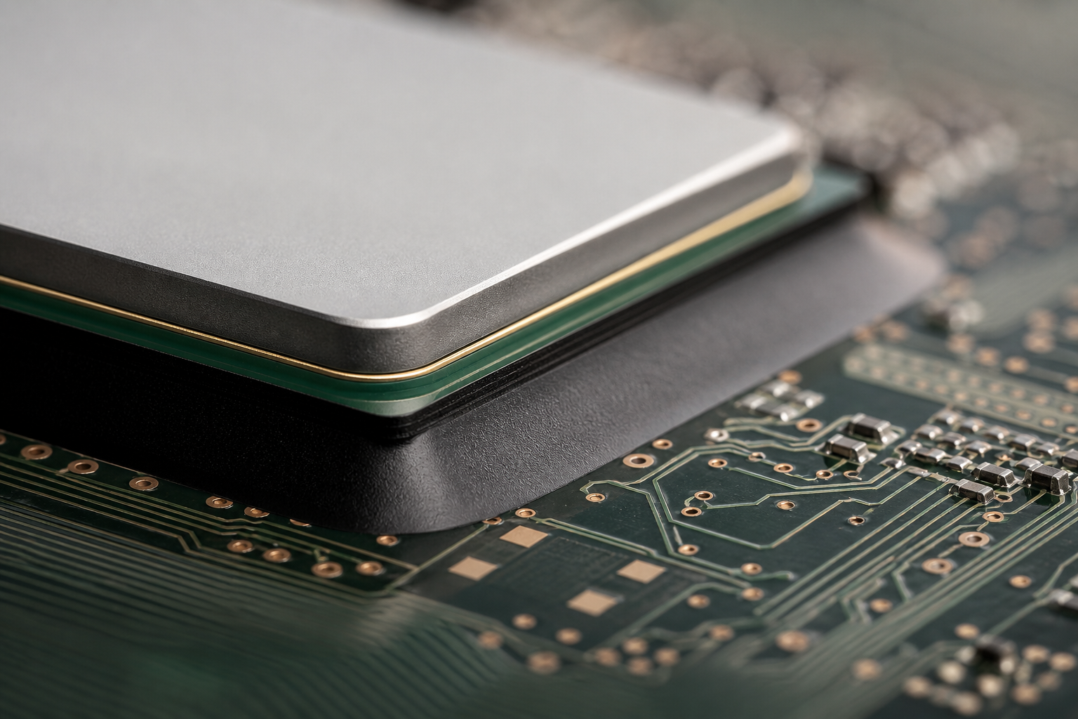
Fillet cosmetics can hide an empty interior. Metrology has to look through, not only around.
Metrology that can carry a disposition
Plants that treat underfill as a real gate tend to combine:
| Method | What it is good for | What it is not | | --- | --- | --- | | Scanning acoustic microscopy (CSAM/SAM) | Void maps at interfaces, production sampling | Instant 100% takt on every unit without a plan | | X-ray / CT sampling | Dense metal-shadow context, selected failure analysis | Cheap daily screen for every lot | | Electrical / thermal screens | Downstream effects | Root-cause map of where polymer is missing | | Process SPC on dispense and cure | Preventing voids | Proving a suspicious lot is empty |
The industrial rule is disposition before mythology: define maximum void area/class by package family, sample rates by risk, and a hold path that does not default to “ship, watch field.”
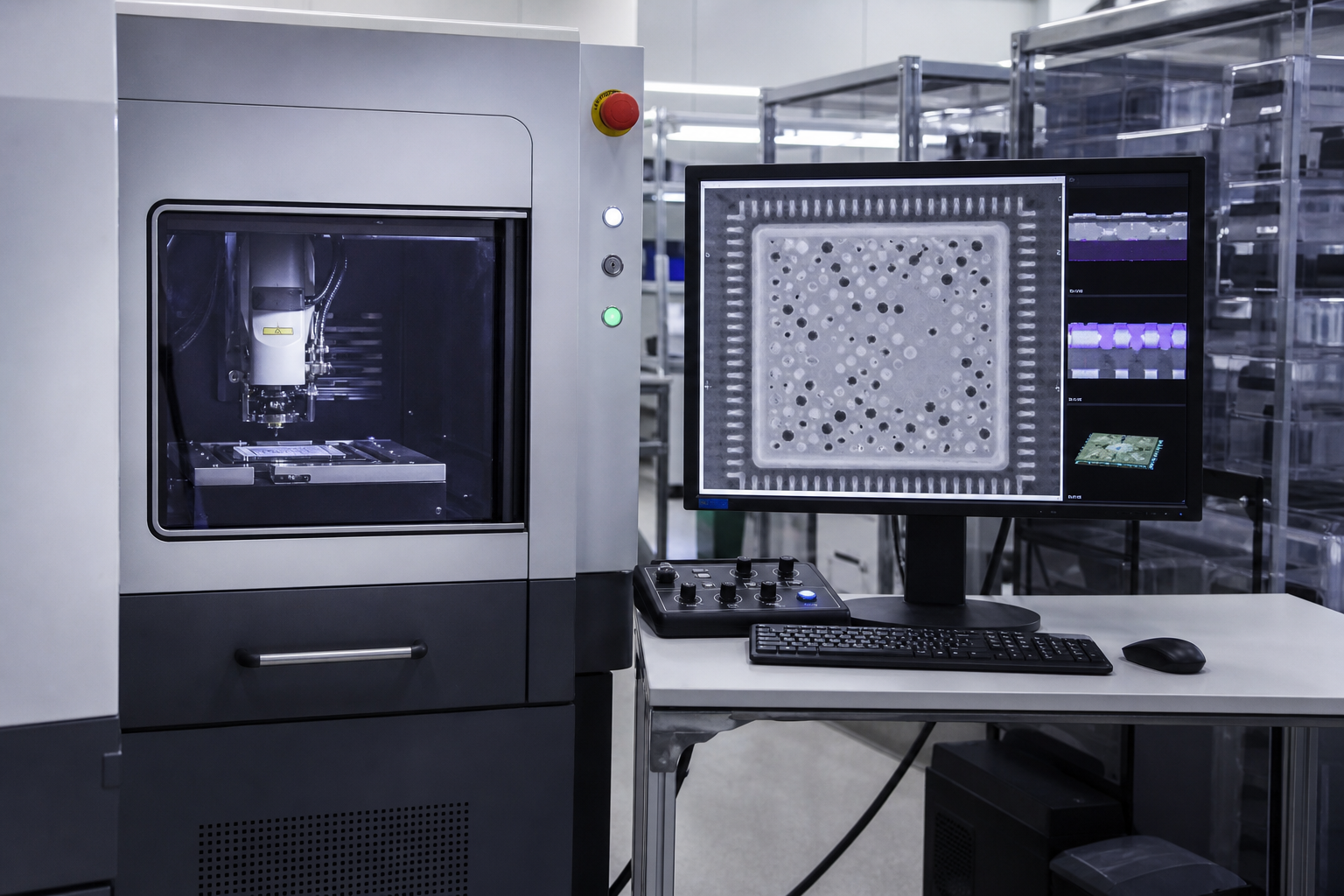
If the void map cannot stop a lot, it is a screensaver.
Governance that keeps packaging honest
- Freeze underfill material, dispense recipe, and cure profile as one controlled set—not three tribal owners.
- Tie void metrology lots to MES genealogy for substrate, bond, and underfill shot IDs.
- Recheck void criteria when die size, bridge count, or substrate stack changes—even if the “same” resin part number is used.
- Ban the sentence “voids are normal at the corner” without a quantified acceptance window and a reliability owner.
Adjacent fences
Hybrid bonding owns interface yield for HBM stacks. Substrate warpage owns shape before attach. Package test and burn-in own outgoing electrical/thermal screens. Glass-core and ABF briefs own materials supply. This page owns underfill integrity as a reliability gate. Do not celebrate a bonding milestone and discover voids only in the RMA lab.