
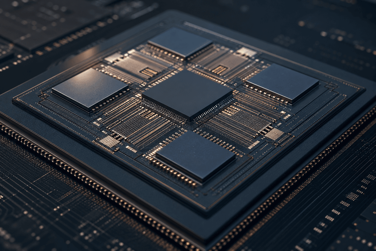
Chiplet architectures chase density and export workarounds. Hybrid bonding gates HBM stacks. CXL pools memory across servers. CPO and LPO move optics. What still decides whether multi-die AI packages interoperate is the die-to-die contract: UCIe and related standards for PHY, protocol, and compliance that packaging houses must actually meet.
Foundries, OSATs, and IP vendors are treating UCIe readiness as a shipping requirement—retimer budgets, bump maps, and test hooks included—not a conference slide.
The industrial point is interoperable chiplets that pass compliance. A custom die-to-die link that only one partner speaks is a captive redesign tax.
What UCIe changes
- Standard PHY and protocol lanes — Multi-vendor die mixes become purchasable.
- Packaging design rules — Bump pitch, channel length, and power delivery aligned to the standard.
- Compliance and test hooks — Bring-up that does not reinvent every program.
What still fails
Calling any multi-die module “UCIe” without compliance evidence. Ignoring thermal and power envelopes of dense die-to-die fabrics. This is not CXL rack memory pooling, not hybrid bond HBM yield alone, not glass vs ABF substrate races, and not CPO optics fabrics.
What to watch next
- Which AI packages publish UCIe compliance paths into volume.
- OSAT tooling and test coverage for standard die-to-die links.
- Whether proprietary links shrink as UCIe ecosystems mature.
Chiplets promise mix-and-match silicon. UCIe decides whether the mix plugs in without a science project.