
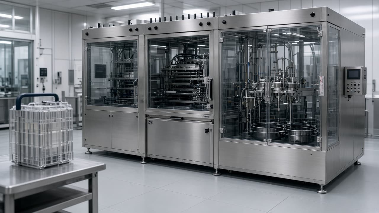
Photoresist spin coating leaves a thicker ridge at the wafer edge—the edge bead. Edge-bead removal (EBR) on the coater/developer track dissolves or rinses that ridge so handling, clamps, and later modules do not flake polymer into the pattern area.
Bevel etch after films and plasma ash for strip are other modules. Here the subject is EBR hardware and recipe honesty on the track.
What fails first
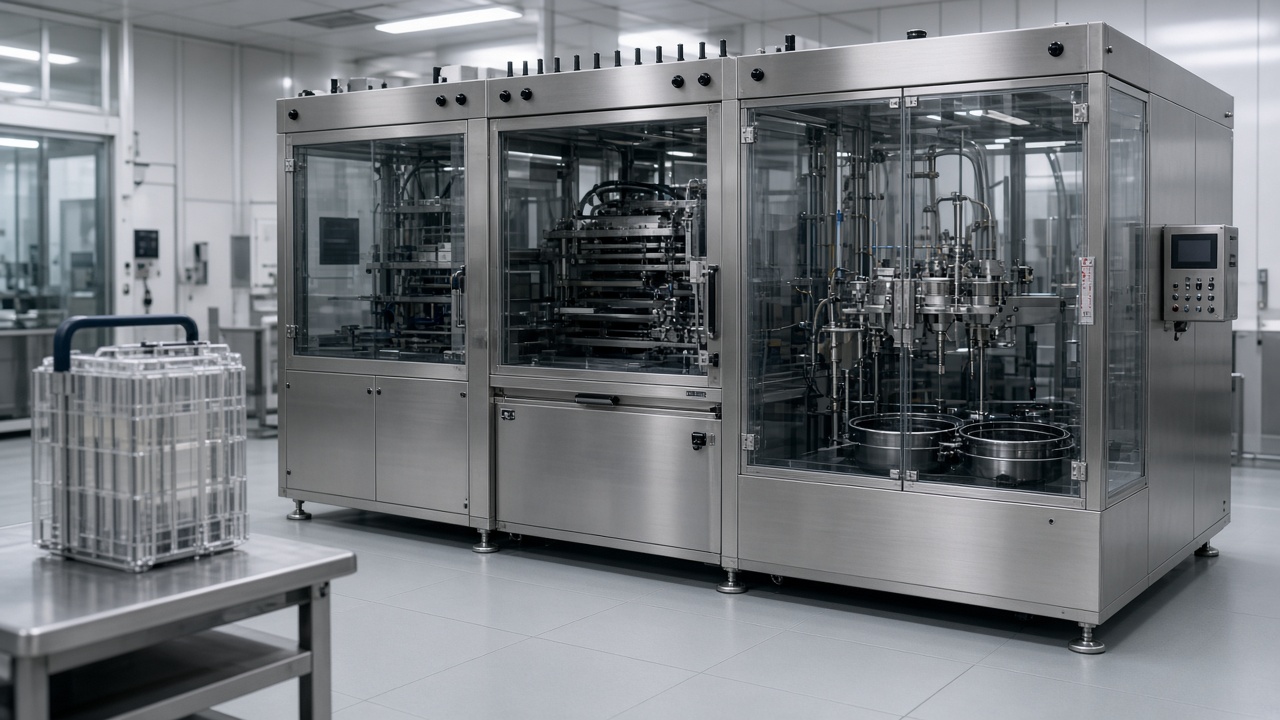
Mis-aimed EBR nozzles paint solvent onto the active die or miss the bead. Wrong solvent or exhausted bottle purity leaves residue that becomes particle adders at scan. Spin speed and dispense timing that drifted after a cup clean change the bead height the recipe still assumes. Back-side rinse and edge rinse that fight each other splash and redeposit.
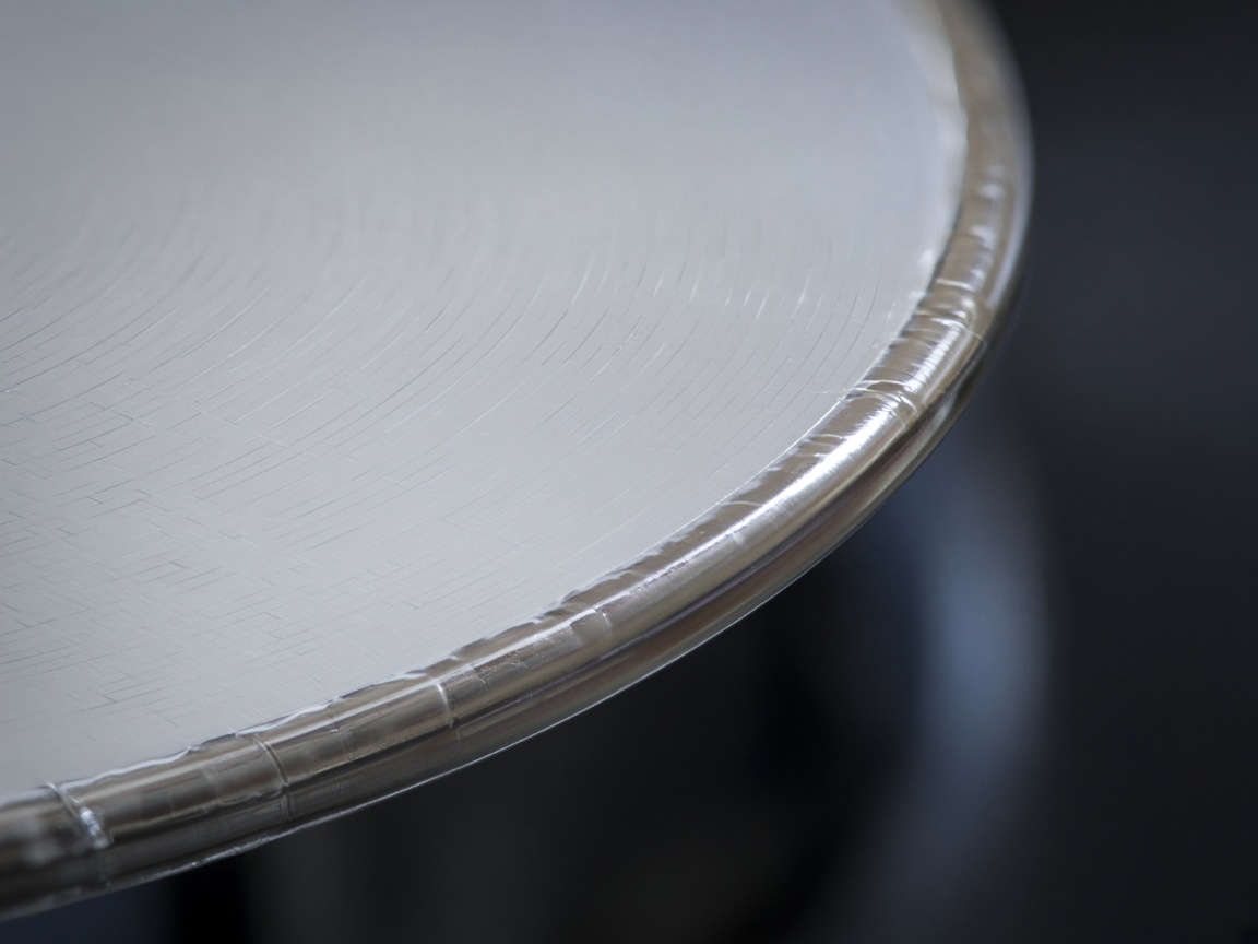
Metrology that only reports center thickness will not catch a bead problem. Edge exclusion maps, visual edge inspection, and particle counts after coat are the early signals. After nozzle change or solvent lot change, run a golden wafer edge check before releasing the track to production lots.
If edge die yield falls while center CD looks fine, walk the EBR cup before you rewrite the etch recipe.