
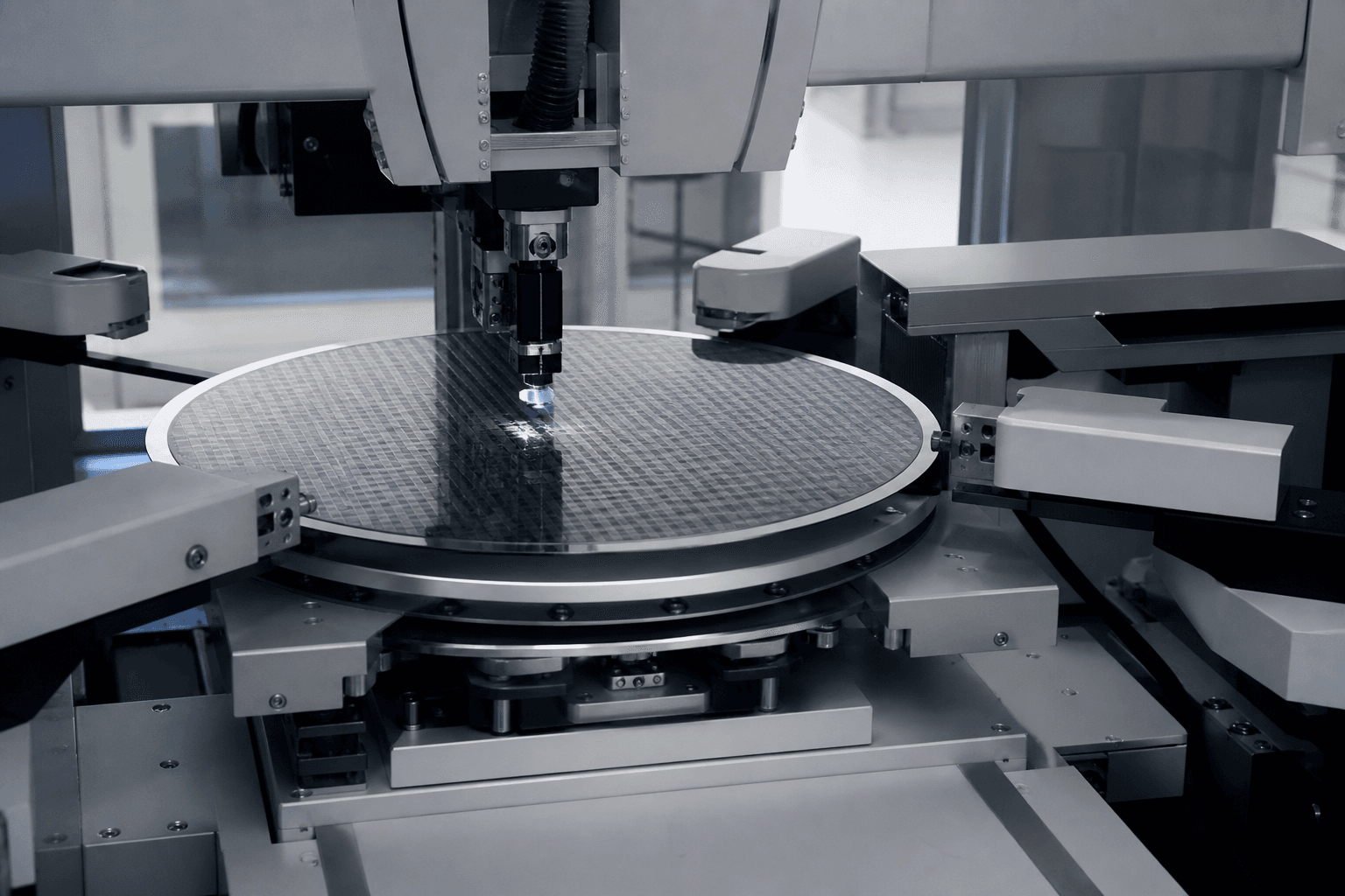
A 300 mm wafer is never a perfect plane. Stress from films, backside films, grind, and thermal history bend it into a bowl, a saddle, or a higher-order shape that the scanner must still flatten against an electrostatic or vacuum chuck. When bow and warp exceed what the chuck and the focus system can correct, the failure is not "mysterious defocus." It is geometry the previous step wrote into the substrate.
Package-substrate warpage is a different problem with different metrology. This is the silicon wafer that enters lithography, etch, and CMP—the disc that still has to sit flat for depth of focus measured in tens of nanometres.
Bow, warp, and what the tool reports
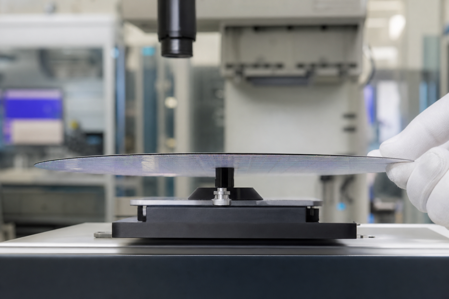
Bow is often summarized as a center-to-edge height relative to a three-point reference. Warp captures more of the free-shape deviation. Both matter. A wafer that looks acceptable on a single bow number can still have local shape that eats the focus budget at the edge dies the customer cares about.
Measurement must know the wafer state: free-standing versus chucked, frontside versus backside reference, and whether a film stack is present. Comparing a free bow from supplier incoming to a chucked shape on the scanner without stating the method is how engineering arguments never close.
Where stress is written
Backside films and asymmetric stacks are classic bow drivers. A deposition that was "in thickness spec" can still move shape if stress is uncontrolled. High-temperature steps and cool-down rates lock in residual stress. Edge trim and backside grind change the mechanical boundary. Each of those steps should either measure shape or inherit a proven window from the last qualification—not wait for the litho tool to alarm on focus residuals.
Incoming bare wafers also vary by vendor and by cassette position in a boat that saw uneven heating. A lot that fails litho focus in a pattern matching one supplier lot is a materials story before it is a scanner story.
Gates that pay for themselves
Put a shape gate where the cost of a miss is highest: after high-stress film, after backside processing, and before critical High-NA or tight-overlay layers. The gate is not a vanity SPC chart. It is a disposition: rework (if the process allows), special chucking/recipe, or scrap—before the lot occupies scanner hours.
Correlate scanner focus residual maps and overlay signatures with pre-litho shape maps. When they align, stop rebuilding the exposure recipe to chase substrate geometry. Fix the stress or the gate.
What chamber and litho matching should ask
Before two scanners are declared mismatched on focus, ask whether the lots they saw had the same bow distribution. Matching tools on wafers that arrive already differently shaped is matching noise.
Wafer shape is a process output of everything that touched stress. Lithography is where that output becomes yield. Measure it as an input, not as a post-mortem.