
Plant systems · 28 Jul 2026
Spare-bin autopsy: what dead PLC cards say about your migration runway
Firmware end-of-support, orphaned I/O families, and counterfeit-risk spares decide whether a controller failure is hours or weeks—plant controls obsolescence story, not passive OT discovery logs, not OPC UA marketing, not MES orchestration slides.
Read more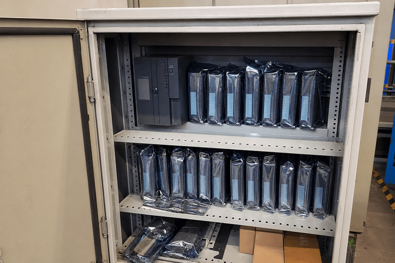
Plant systems
Semiconductors
Semiconductors
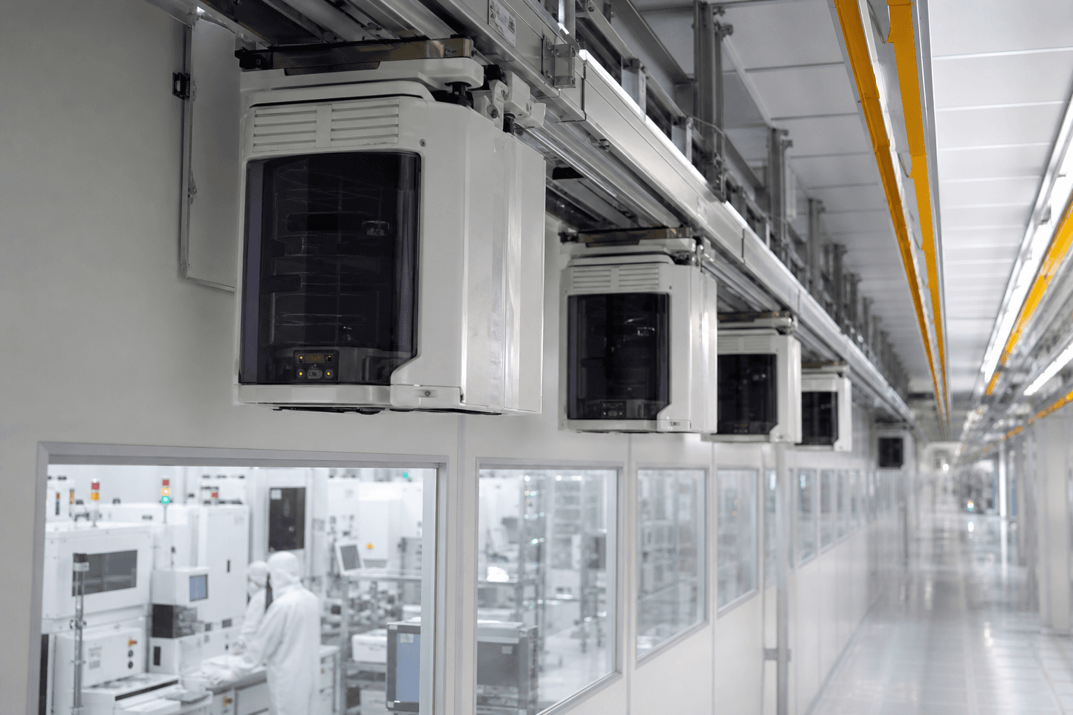
Travelogue of FOUP #A-7741: contamination is a route, not a particle myth
Carrier history, AMHS handoffs, and loadport discipline decide whether wafers inherit foreign particles—semiconductor logistics-contamination story, not AMC detective timelines, not UPW purity loops, not photoresist track cold chain.
28 Jul 2026
Semiconductors
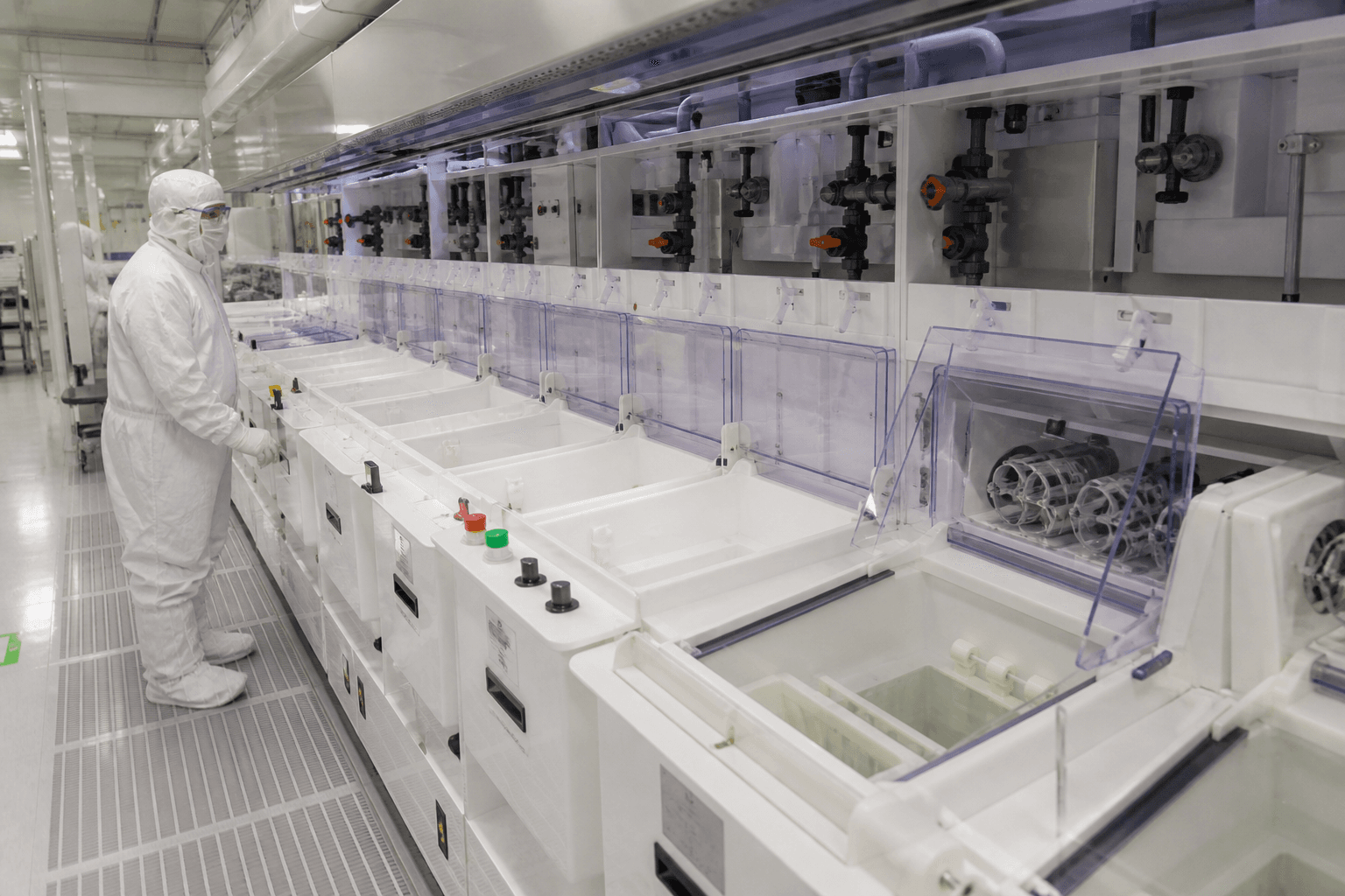
Lab notebook: wet-bench bath #7 and the lifetime nobody logged
Bath age, spike chemistry, and changeout triggers decide particle and etch drift—semiconductor wet-process notebook, not UPW loop purity, not CDA dew point, not photoresist track logistics.
28 Jul 2026
Semiconductors
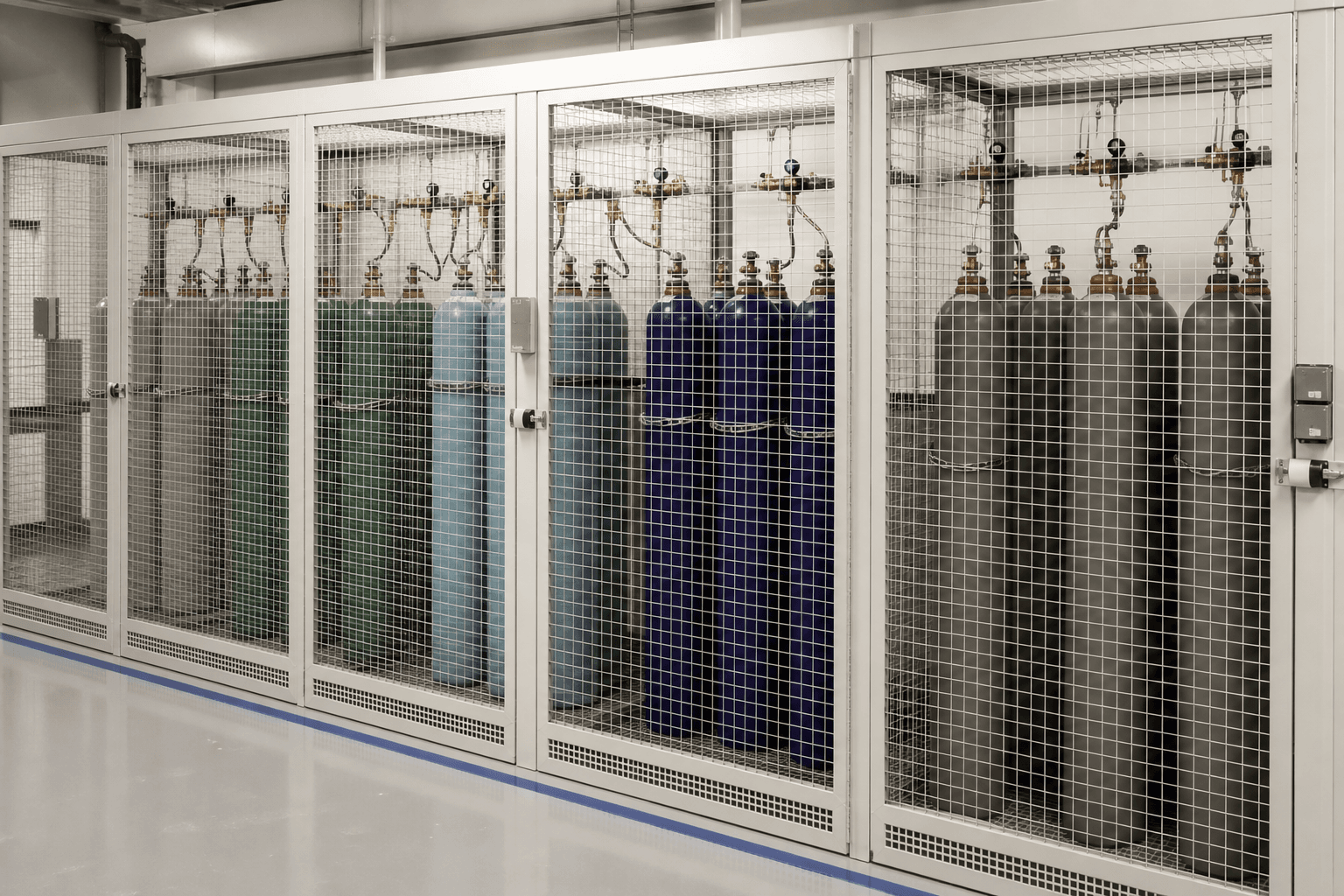
War-room transcript: neon, helium, and the fab that thought gas was a PO
Cylinder allocation, purity grades, and dual-source lies decide litho and etch uptime when specialty gases tighten—semiconductor materials capacity story, not photoresist cold chain, not CMP slurry totes, not dry-vacuum pump rebuilds.
28 Jul 2026
Semiconductors
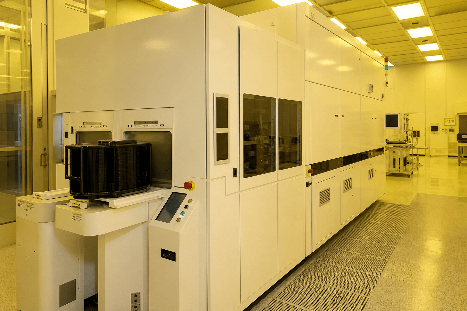
Follow the dose: ion implant as a closed measurement chain
Beam current, Faraday cups, charge neutralization, and dose SPC decide device parametric health—semiconductor metrology-control story, not photoresist track logistics, not High-NA stitching, not dry-vacuum pump reliability.
27 Jul 2026
Semiconductors
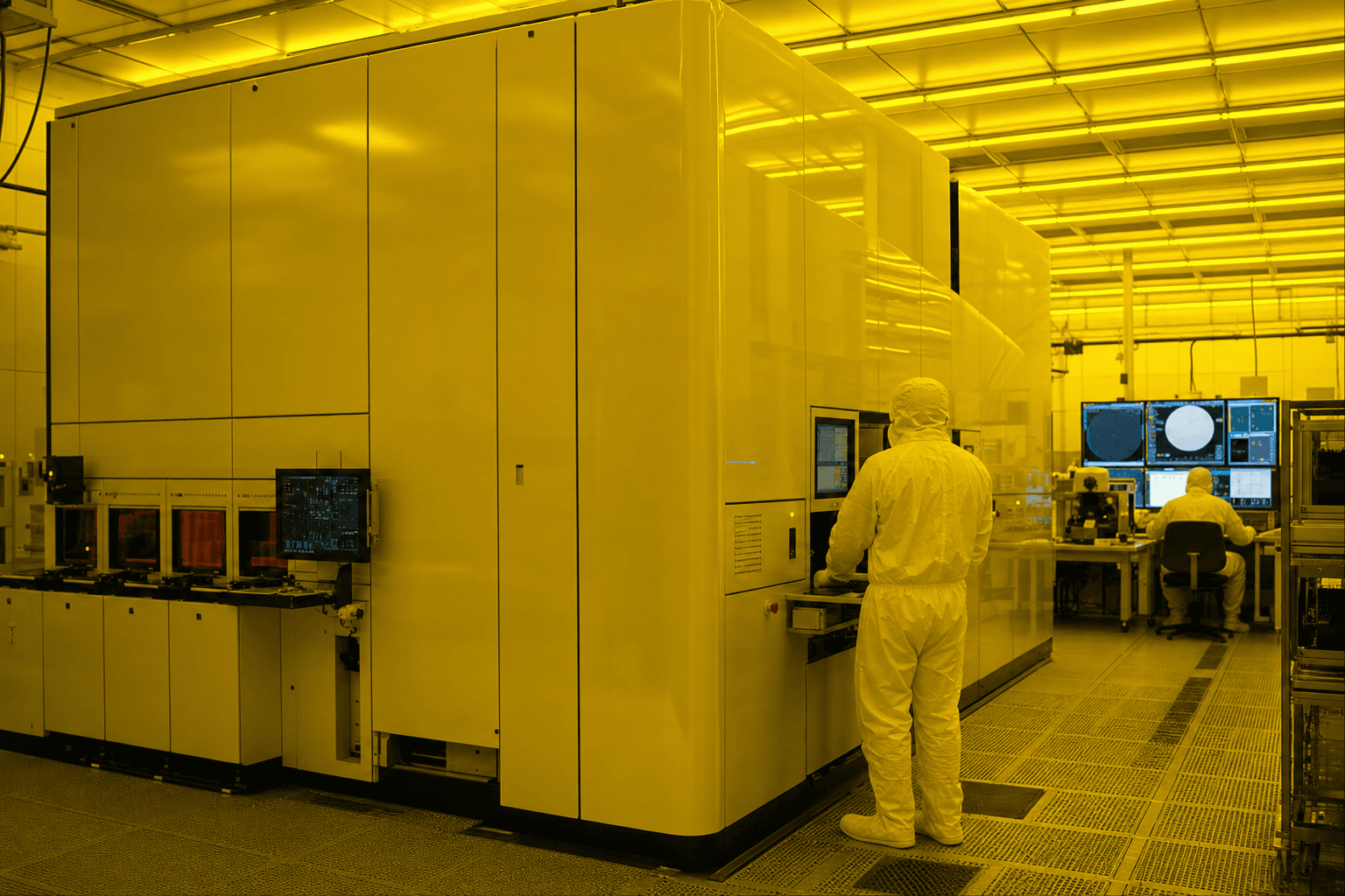
High-NA EUV fails as stitching and depth-of-focus, not as a scanner brochure
Field stitching, thin-resist DOF, and mask–etch co-optimization decide High-NA yield windows—semiconductor process story, not High-NA tool overviews, not pellicle logistics, not photoresist track cold chain.
25 Jul 2026
Semiconductors
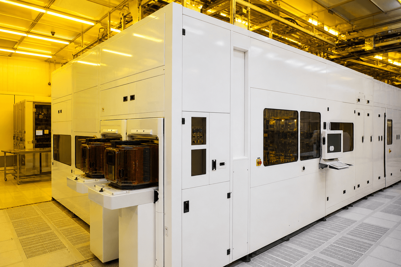
The track coater is a supply chain: when resist logistics fail, litho waits
Photoresist cold chain, dispense health, and coat uniformity decide lithography queue time—semiconductor consumables story, not EUV pellicle supply, not AMC hunts, not dry vacuum pumps.
24 Jul 2026

Semiconductors
The dry-pump war room: when tool vacuum becomes a fab capacity constraint
Dry vacuum pumps, forelines, and abatement decide etch/CVD uptime—semiconductor utilities story, not CMP slurry totes, not AMC hunts, not nitrogen blanketing.
23 Jul 2026
Semiconductors
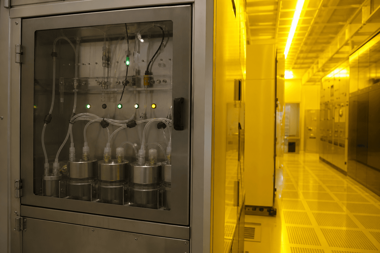
Hour 0 to week 2: how an AMC hunt actually clears a lithography bay
Airborne molecular contamination is a detective timeline for resists and optics—not CMP slurry logistics, not EUV pellicle supply, not cleanroom HVAC brochure math.
22 Jul 2026

Semiconductors
CMP slurry is a process chemical supply chain wearing a tote label
Particle size, pad pairing, and dual-source logistics decide polish yield—procurement timeline for fabs, not another substrate or mask story.
21 Jul 2026

Semiconductors
EUV photomask and pellicle supply becomes the hidden lithography gate
Mask-shop capacity and pellicle yield own scanner utilization after the tool is installed—adjacent to High-NA CapEx and ABF substrates, focused on reticle logistics.
21 Jul 2026
Semiconductors
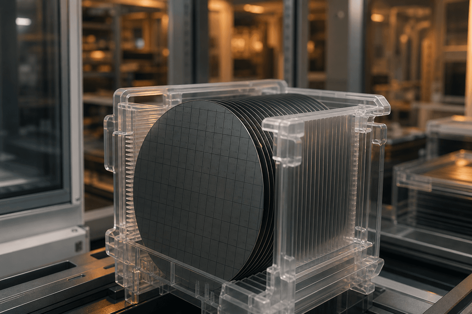
SiC wafer supply becomes the bottleneck behind power device ramps
Boule-to-wafer capacity, defect density, and diameter transitions—distinct from SiC/GaN device headlines, SST racks, and industrial drive installs.
20 Jul 2026

Semiconductors
Substrate warpage metrology becomes the quiet gate for large AI packages
Flatness measurement and process control on big organic and panel carriers—distinct from ABF capacity headlines, glass-core bets, and package test floors.
20 Jul 2026
Semiconductors
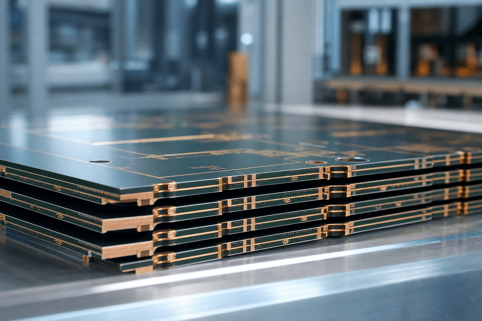
ABF organic substrates remain the volume gate while glass pilots
Build-up ABF capacity and yield still ship most AI packages—distinct from glass-core bets, CoWoS/CoPoS lines, and package test floors.
19 Jul 2026
Semiconductors
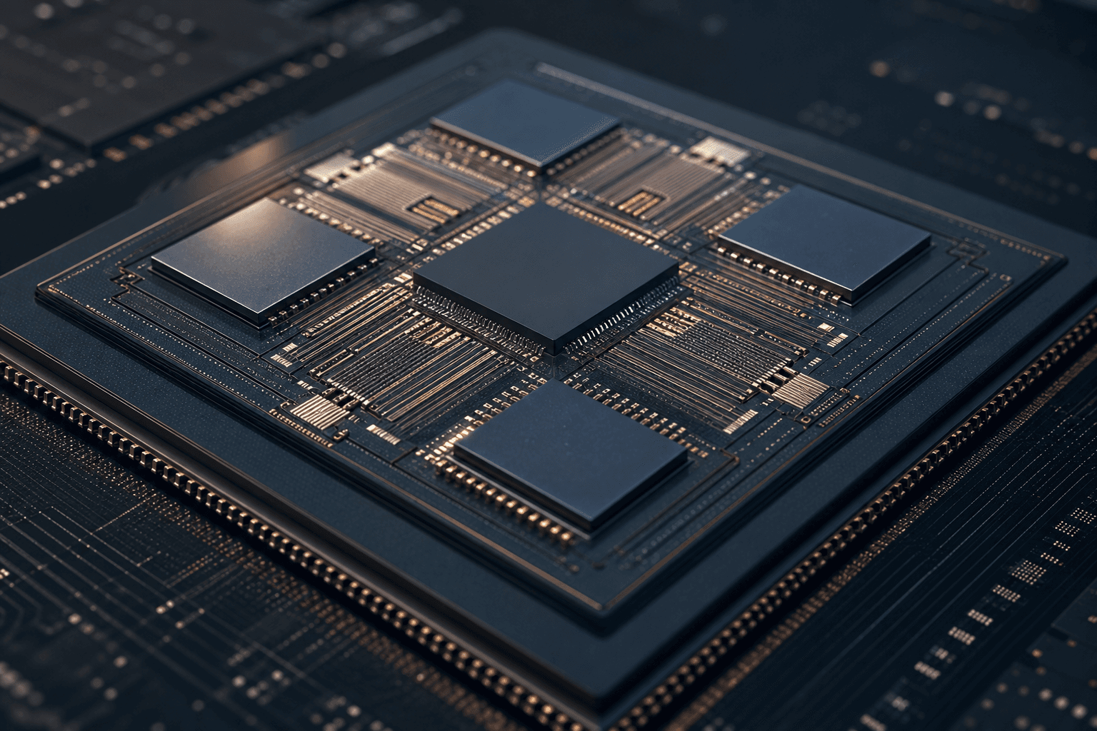
UCIe turns chiplet interconnect from slideware into a packaging contract
Die-to-die standard compliance and PHY constraints—distinct from chiplet export narratives, CXL pooling, hybrid bond yield, and CPO/LPO optics.
19 Jul 2026

Semiconductors
Package test and burn-in become the AI packaging throughput gate
Handler, socket, and burn-in capacity now limit advanced AI packages—downstream of CoWoS, hybrid bond, and glass substrates.
17 Jul 2026
Semiconductors
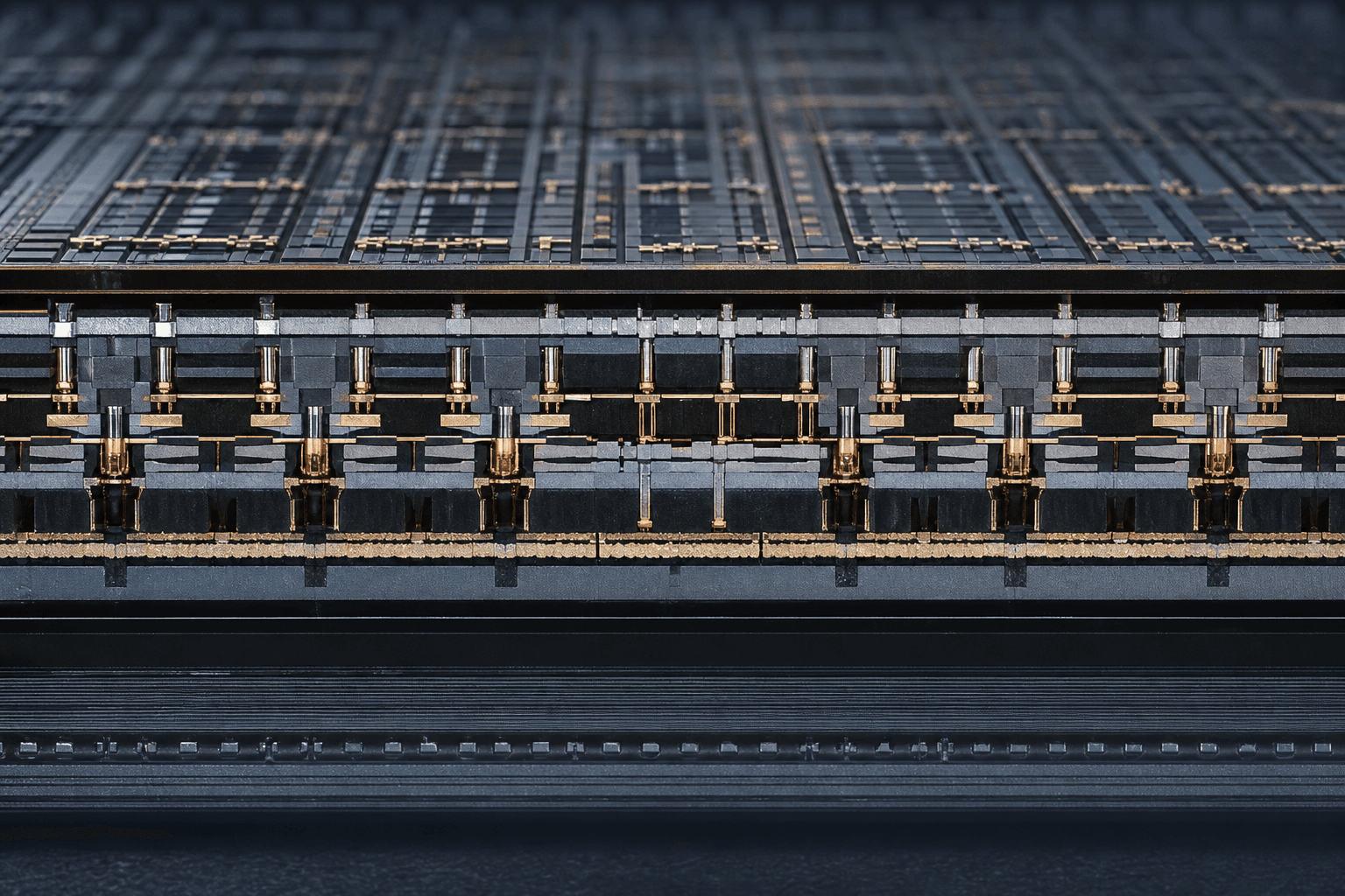
CFET stacking becomes the density bet after nanosheet GAA
Complementary FET vertical stacking targets continued logic shrink—distinct from GAA risk ramps, hybrid-bonded HBM, and advanced packaging races.
11 Jul 2026
Semiconductors
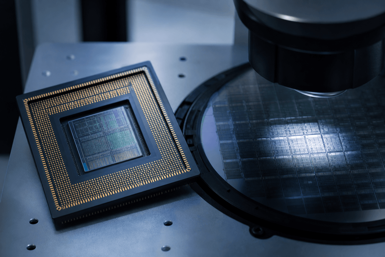
Processing-in-memory targets AI’s data-movement tax
PIM and near-memory compute aim to cut HBM shuttle energy for inference and embedding workloads—architecture relief, not another packaging or bonding race.
06 Jul 2026
Semiconductors
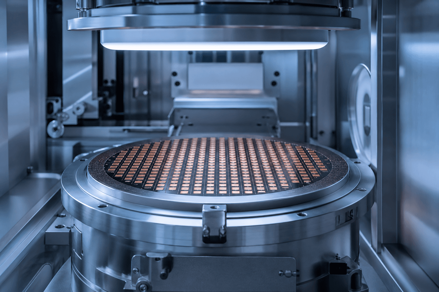
Hybrid bonding becomes the yield gate for AI HBM stacks
Cu-Cu and hybrid bonding move HBM and logic closer—capacity follows bond yield and cleanroom CapEx, not only wafer starts or substrate roadmaps.
01 Jul 2026
Semiconductors
Glass-core substrates become the next AI packaging materials race
Through-glass vias and glass cores are leaving the lab—pilot lines and JVs target 2026–27 qualification as organic substrates hit warpage and size limits on large AI packages.
28 Jun 2026

Semiconductors
GAA nanosheet logic moves from roadmap slide to risk production
Gate-all-around transistors are no longer a future node promise—18A-class flows with RibbonFET-style devices are in risk production, pairing GAA with backside power for AI-era density.
24 Jun 2026

Semiconductors
LPO optics bridge AI fabrics before full CPO lands
Linear and other pluggable optical paths are taking 2026 volume while co-packaged optics mature—lower power than copper, less integration risk than CPO, and a real procurement choice for scale-out.
19 Jun 2026

Semiconductors
CXL memory pooling becomes AI’s capacity bypass
When HBM and GPU packages hit cost and supply walls, CXL fabrics let racks share commodity DRAM—slower than HBM, but cheaper capacity that stops buying compute just to get memory.
14 Jun 2026

Semiconductors
Chiplets and 3D stacking become the export-control workaround
With advanced EUV access constrained, designers push performance through packaging—chiplets, hybrid bonding, and vertical stacks—turning architecture into a geopolitics strategy.
09 Jun 2026
Semiconductors
HBM4 turns memory into the AI supply-chain race
Mass production and early HBM4E samples in 2026 reset who can feed the next accelerator wave—base-die process, stack height, and customer qualification now matter as much as DRAM bits.
04 Jun 2026
Semiconductors
Backside power delivery becomes an AI-node design constraint
Routing power from the wafer backside frees front-side interconnect for signals—but process complexity, thermal paths, and yield learning decide who ships it first.
30 May 2026

Semiconductors
High-NA EUV becomes a fab CapEx and process decision
0.55-NA EUV tools are entering qualification for sub-2nm work—but cost, throughput, and whether multipatterning on 0.33-NA still wins remain the real roadmap questions.
25 May 2026

Semiconductors
Co-packaged optics moves from demo to AI fabric constraint
As switch ASICs and GPU clusters push past copper limits, CPO promises lower energy per bit—while yield, lasers, thermal design, and serviceability decide real adoption.
23 May 2026
Semiconductors
From CoWoS to CoPoS: panel packaging enters the AI roadmap
Wafer-level advanced packaging is still the workhorse, but panel-level platforms are being qualified to stretch size, cost, and throughput for the next wave of accelerators.
21 May 2026
Semiconductors
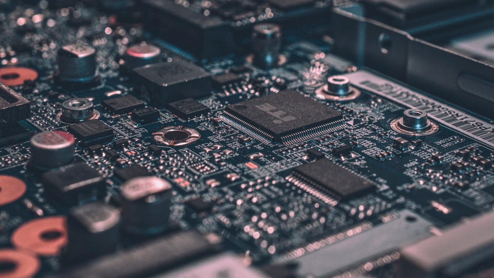
Advanced packaging and HBM now set the AI chip pace
Leading-edge wafers are only half the story. CoWoS-class packaging and high-bandwidth memory allocation decide which AI accelerators reach volume.
19 May 2026