
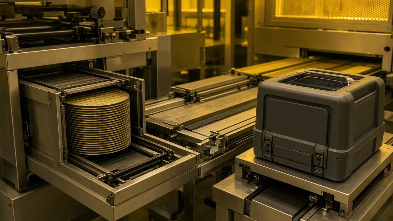
The scanner finishes. The wafer sits. Acid from the exposure event keeps moving in the resist film until post-exposure bake (PEB) locks the profile. That waiting interval—post-exposure delay, PED—is process time. When FOUPs stack between the exposure tool and the PEB plate because the track or AMHS is busy, critical dimension walks in a direction that looks like “scanner drift” until someone plots CD against expose-to-bake minutes.
PEB hot-plate uniformity owns temperature range across the wafer once bake starts. Fab Q-time between etch and film owns surface chemistry after plasma. This page is the expose → PEB queue: the clock that starts when the latent image exists and ends when the plate holds the wafer at bake temperature.
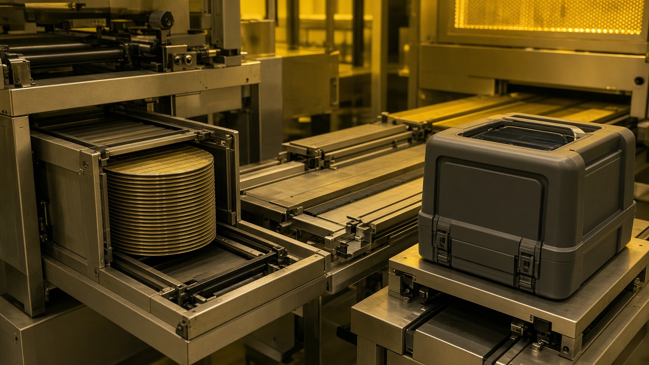
For many CA resists, PED sensitivity is real enough that process windows quote a maximum delay—and sometimes a minimum—between exposure and PEB. Ambient acid quench, humidity, and airborne base contamination in the bay can shrink that window without any recipe edit. A lot that “ran the same dose” after a forty-minute loadport wait did not run the same process as a lot that moved in five.
Timestamps that matter: exposure complete (or last die exposed for the lot), PEB start on the plate, and any intermediate stocker or loadport dwell. MES “lot move” alone is too coarse. If the inhibit only paints yellow on a WIP board, planners will waive it for a hot lot. The control that works is refusal: the PEB module or track host will not accept the lot past the PED limit without a documented recovery—re-expose path, strip and recoat, or scrap disposition—owned by lithography process, not by dispatch utilization.
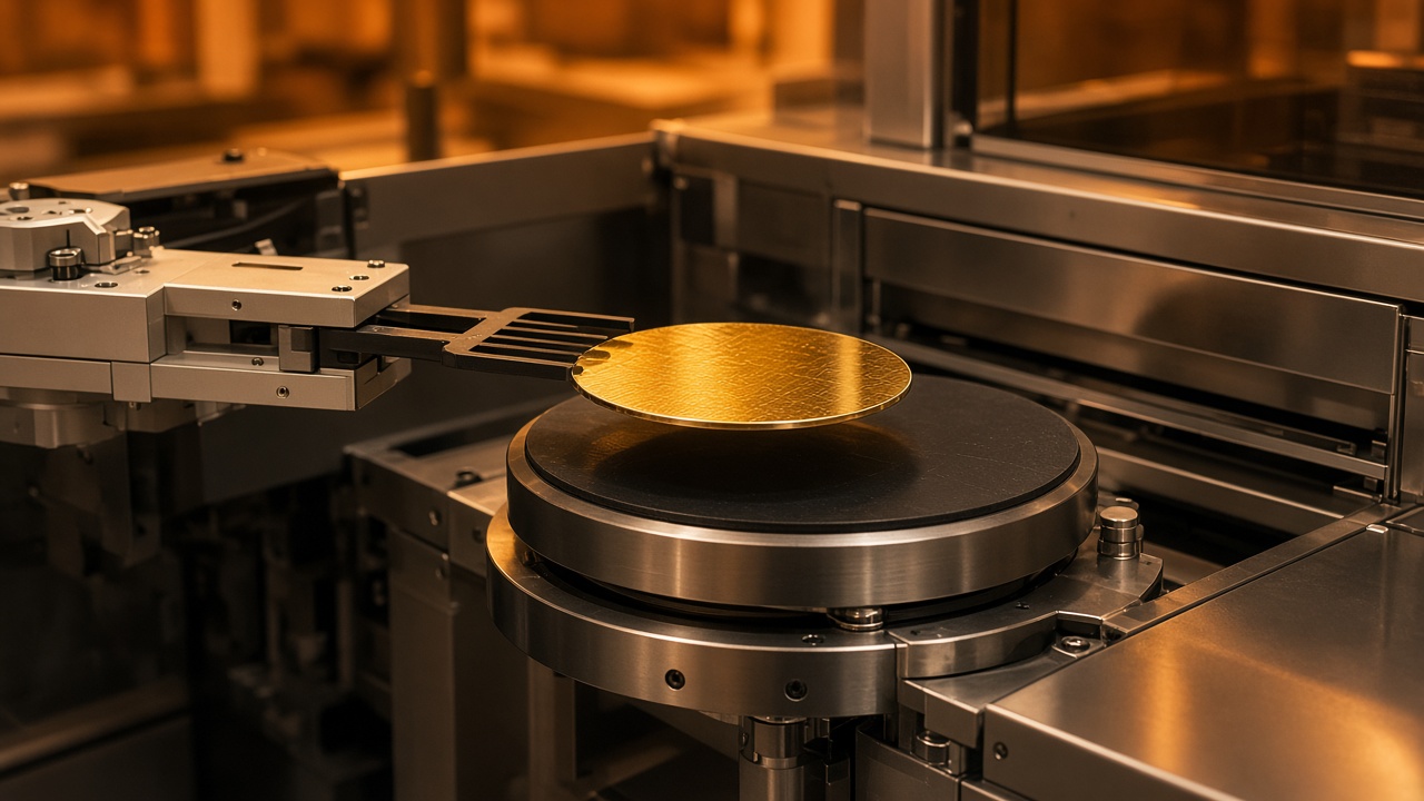
When CD signatures cluster on lots with long post-exposure dwell and quiet focus/dose history, hold against PED genealogy before funding another energy ladder. The track owns whether the latent image still matches the model the scanner thought it printed.