
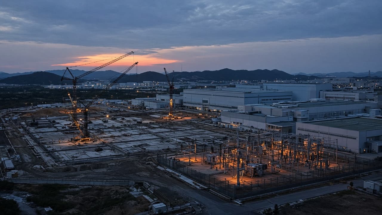
Seoul Economic Daily reported on 4 November that Samsung has decided to place 2-nanometer and 4-nanometer foundry capacity on land at its Giheung campus where the Samsung Advanced Institute of Technology building (SR5) and an engineering-college building (CDI) finished coming down last month. Citing industry sources, the paper describes a Kairos complex, a green building and a substation, with Samsung E&A as EPC contractor, and a first fab raised in four phases the way the newer Pyeongtaek plant was.
The constraint is narrower than “another leading-edge fab.” HBM4 core dies already run at Hwaseong and Pyeongtaek. Base dies for that generation, on a 4-nanometer foundry flow, occupy only some of those lines. Giheung opened in 1983 and is still the mature-node campus: Line 6 on 200 mm wafers for image sensors, display drivers and power devices; Line S1 for mobile and automotive logic. Project Kairos, as the paper frames it, would drop a process generation onto a site that has not run one. The same account says the task force also means to turn part of Line 6 into advanced packaging—the step that makes a stack out of the dies.
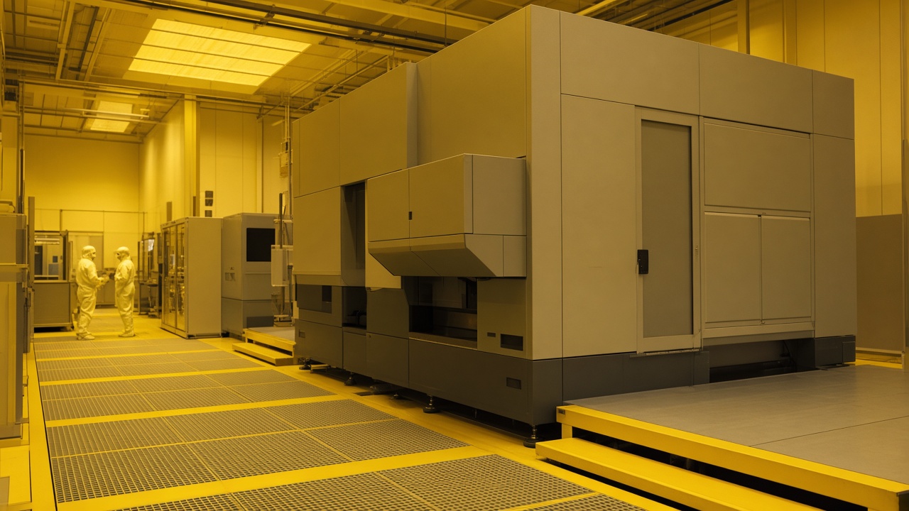
The won figures are estimates, not a disclosed budget. The Kairos fab itself is put at about 25 trillion won. Sources told the paper that internal purchase quotes cover several dozen EUV scanners, on the order of 8 to 10 trillion won. Cleanroom plus the non-lithography toolset pushes the sum past 20 trillion; observers cited in the piece, once the Line 6 packaging conversion is included, land near 30 trillion. A quote is not a dock date. The same week, Electronic Times reported that suppliers including ASML, Applied Materials, Lam Research, Tokyo Electron and KLA are closing talks for 2028 tools and, in places, discussing 2029 orders, with some lead times now past two years.
Memory makers are already separating the building from the wafers. EDAILY quoted SK hynix chief financial officer Kim Woo-hyun on raising shells—Yongin and M17 among them—ahead of demand, then opening cleanrooms in phases and installing tools only when volume is real. The same report said Samsung is preparing cleanroom space and choosing later when the equipment goes in. Concrete and output are no longer the same milestone.
The Seoul paper also treats the 2-nanometer line as preparation for an HBM5 base die, which it describes as likely to leave the 4-nanometer process used for HBM4 and for HBM4E—the latter, in the paper’s telling, aimed at mass production next year. That generation timing is the newspaper’s reading. It is not a customer qualification notice.
What can be scheduled is plainer. Core-die output at Hwaseong and Pyeongtaek does not become HBM until a foundry base die and a packaging line exist in the same quarter. Giheung’s cleared pad starts that argument. On the public record, the EUV tools that would settle it are still quotes.