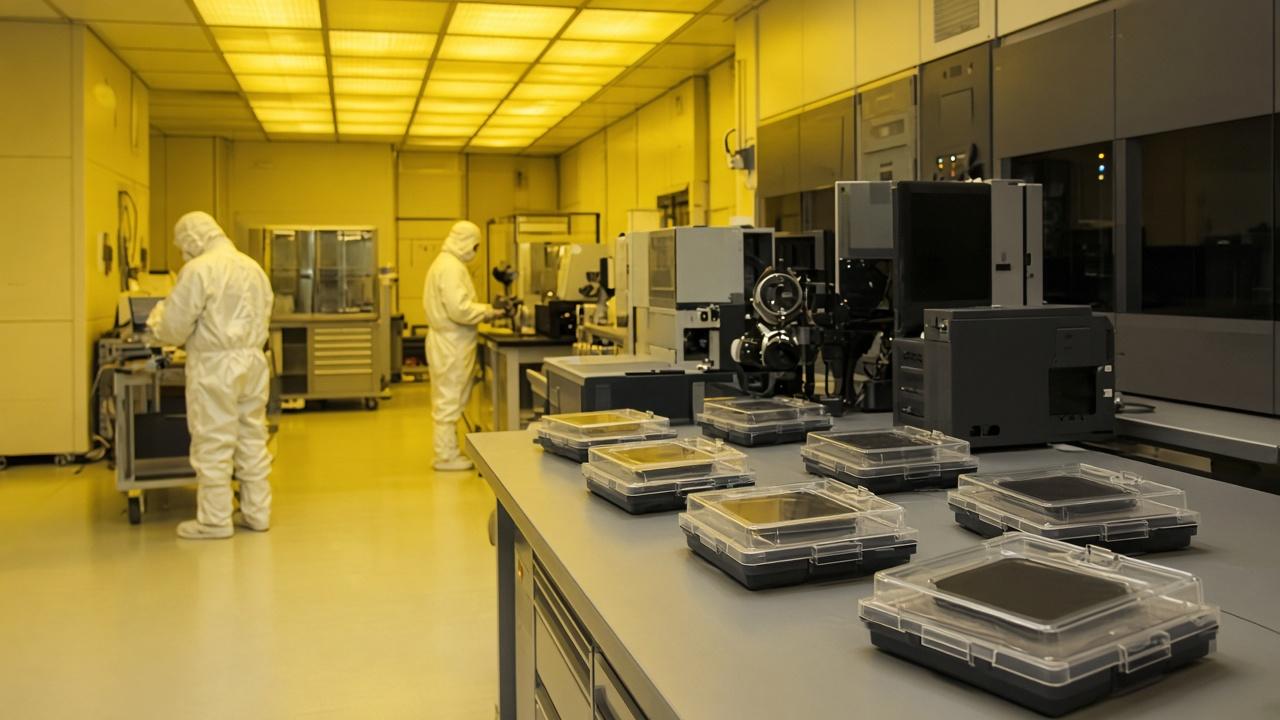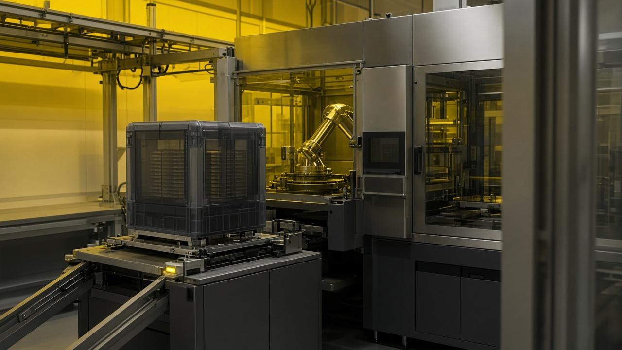
Ed Kaste, senior vice president of GF’s CMOS business, put the requirement first: Physical AI moves intelligence into devices that sense, decide, and act in real time, and that creates a different semiconductor brief than cloud training silicon. GlobalFoundries answered on 9 October 2026 in Dresden by naming FDX Fusion—the next major extension of its FDX fully depleted SOI roadmap—and tying first manufacturing to the same European fab that already runs volume 22FDX.
GF’s language for the first Fusion generation is seven-nanometer-class digital performance, built from substrate engineering, front-end transistor work, and back-end interconnect rather than a jump to leading-edge FinFET. The platform is said to combine RF performance up to 0.5 THz ft/fmax with analog and mixed-signal features, low-leakage operation, in-memory computing, embedded non-volatile memory, and dense logic. Density improvement over first-generation FDX is stated as more than 2×. Those figures are GF’s published expectations. They are not independent silicon results from a named customer tape-out, and “world’s most advanced FD-SOI” plus “first process technology in Europe to deliver single-digit nanometer digital performance” remain comparative marketing lines that this note will not amplify as proven fact.
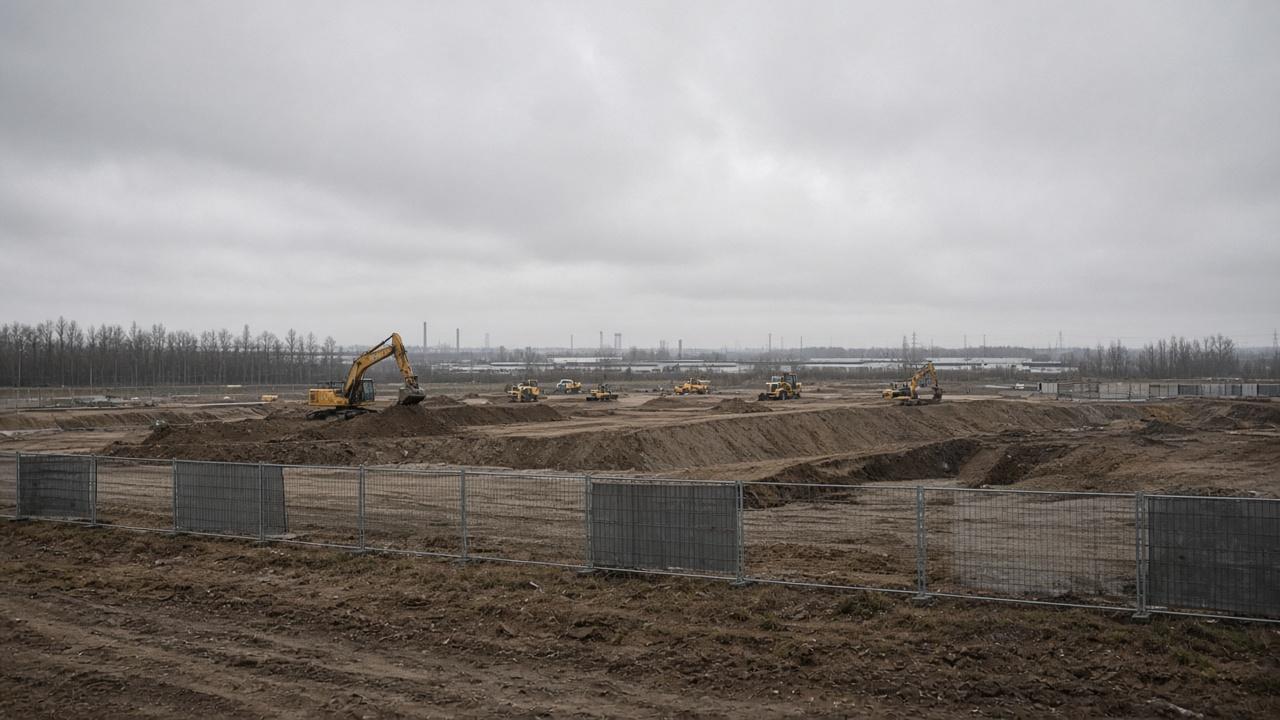
The calendar is clearer than the superlatives. Demonstrator silicon for early customer evaluation is targeted for early 2027. An initial process design kit is planned for mid-2027. Manufacturing of FDX Fusion technology is planned to commence in 2028 at Dresden. That Dresden link is deliberate. The same day GF celebrated the topping-out of its SPRINT expansion: a €1.1 billion investment expected to lift annual capacity at the site to more than one million 300 mm wafers by the end of 2028 under the European Chips Act framework. FDX Fusion development work is also described as intended to run through the upcoming IPCEI Advanced Semiconductor Technologies programme, subject to German federal government approval—so the roadmap and the funding path are not fully decoupled.
Application targets sit in automotive, consumer, and industrial markets: edge inference, robotics, industrial automation, autonomous systems, sensor-fusion architectures, and connected devices. GF says it is already engaged with several customers on early development and evaluation. Named ecosystem comments in the release come from BMW Group (supply-chain resilience framing), Bosch’s Dr. Axel Kaschner (sensing, control, connectivity, edge intelligence for robotics and automation), CEA-Leti’s Sébastien Dauvé (single-digit FD-SOI and the FAMES pilot line), Infineon’s Patrick Press (7 nm-class FDX Fusion for next-generation radar and wireless), NXP’s Lars Reger (trusted, low-power Physical AI), Siemens’ Cedrik Neike (industrial systems), and Tesla’s Karn Budhiraj (edge compute for robotics and autonomous systems). Those are stakeholder statements of interest, not purchase orders with volumes and dates.
Design enablement is part of the pitch: GF’s MIPS and ARC processor IP portfolio, RISC-V ISA support, and application-specific processor design for Physical AI workloads, meant to sit alongside the Fusion PDK so customers are not starting compute architecture from a blank sheet. That matters for edge SoC teams; it does not replace RF characterization, automotive qualification, or package choices that remain with the customer.
GF’s existing FDX base is the commercial context for why Fusion is framed as extension rather than a cold start. The company says billions of FD-SOI chips are already in use across automotive radars and sensors, wireless microcontrollers, display drivers, and front-end modules for SATCOM and 5G. Fusion is meant to keep that RF-and-mixed-signal constituency while adding denser digital and in-memory features for edge AI. STAC—Sense, Think, Act, Communicate—is the workload shorthand GF uses for that brief. Whether a given SoC actually collapses sensing, inference, control, and connectivity onto one Fusion die is still a customer architecture decision; the platform claim is that the process options exist to support that integration without moving to a leading-edge logic node.
SPRINT and Fusion share a campus but are not the same announcement. SPRINT is a capacity and buildings programme: €1.1 billion, topping-out celebrated on 9 October, more than one million 300 mm wafers per year targeted by end-2028, additional capacity aimed at automotive, aerospace, industrial IoT, and defense. Fusion is a process roadmap that intends to use that Dresden capacity once the PDK and process flow are ready. Conflating “fab getting bigger” with “7 nm-class silicon shipping” is the main reading error to avoid. GF also notes optimized process flow and cost structures for rapid prototyping—useful for early customers, not a substitute for high-volume qualification.
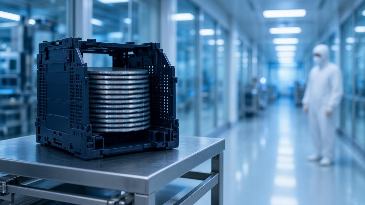
Readers who have been tracking advanced packaging notes should keep this file separate. FDX Fusion is a process-platform and Dresden capacity story. It is not a CoWoS or interposer announcement, not a Malta packaging capacity add, and not a claim that FD-SOI replaces FinFET for high-performance cloud compute. Limits worth repeating: production is planned for 2028, not shipping today; density and 7 nm-class performance are GF expectations; IPCEI AST funding is contingent on German federal approval. The practical observation points for the next year are whether the early-2027 demonstrator arrives on schedule, whether the mid-2027 PDK lists the RF and embedded-memory options customers need, and whether SPRINT’s capacity ramp and Fusion’s process maturity stay aligned. Until those land, the verified core is the 9 October date, the Dresden manufacturing anchor, the 2027–2028 enablement and production windows, the >2× density and 0.5 THz ft/fmax claims as published GF specs, and a clear separation from advanced-packaging news elsewhere in the sector.