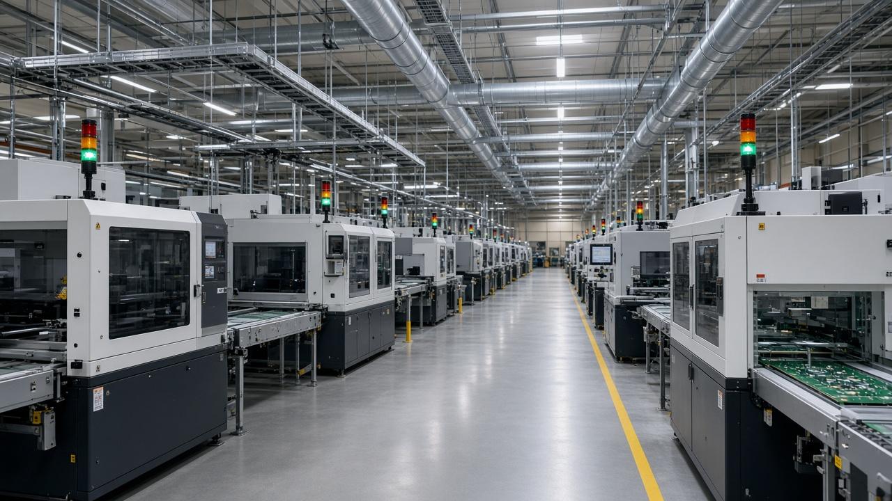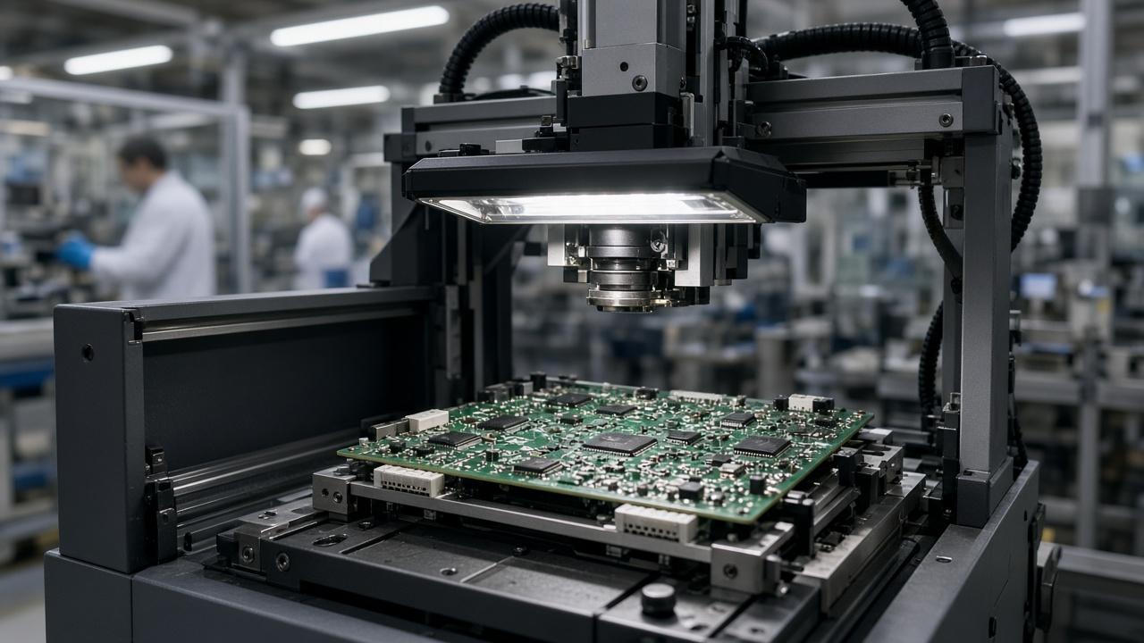
Siemens and NVIDIA announced on 21 October a collaboration to prepare automated optical inspection for printed circuit boards from a product digital twin and synthetic imagery. Siemens is showing the workflow at its Electronics Factory Erlangen in Germany, combining Teamcenter, Process Preparation X, and NVIDIA Cosmos. The subject is electronics assembly inspection, not wafer-defect inspection in a fab.
The preparation path is ordinary manufacturing data first. Board design, bill of materials, and component libraries live in Teamcenter. Process Preparation X turns that into a digital representation of the populated board. Cosmos then helps generate photorealistic reference images and synthetic production conditions so inspection programming can begin before a physical golden board is available. For plants that change board revisions often, the hard part is usually mapping the right revision to the right recipe—not inventing pixels alone.
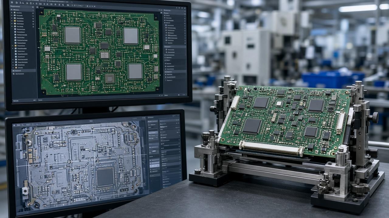
Siemens stated project targets of up to 85 percent less manual engineering effort in inspection-program generation, roughly 40 percent fewer false calls, and more than 5 percent first-pass yield improvement. Those are targets for the collaboration, not independently measured results available to every line. A second AI-assisted review is meant to help sort optical-inspection flags into real defects versus false calls. Detecting a suspicious condition and deciding whether to intervene remain two different judgments; cutting false calls only helps if true defects still leave the station.
Berea’s assembly cameras, covered earlier, asked whether a discrete assembly step happened. Erlangen asks whether the inspection program can be prepared from design data before hardware exists, and whether a second look can thin false alarms. Without a published benchmark set, pricing, or general rollout date, the operational claim to carry is earlier preparation—not a guaranteed yield delta.